(PCBs) are made up of wiring, which carries a charge.
One such conductor used in many printed circuit boards is copper.
Of all the conductors, copper does the best to maintain a reasonable amount, correctly powering the printed circuit board.
One problem with copper is that it can be exposed to elements if unprotected.
If exposed to any form of the atmosphere, copper will oxidize.
It can make it difficult to bond with whatever it is soldered to and decrease the rate and quality of its conducting qualities.
One method to address this is to cover the untapped copper surface and create a solder mask with resins and paints.
There is a better way to do this before copper oxidation and decomposition. It is called PCB tinning.
PCB tinning is a preventive method that will ensure that copper traces last as long as possible before any oxidation or corrosion occurs. Come with me and learn more.
Contents
- 1、PCB Tinning
- 1.1 Benefits of PCB tinning
- 1.2 Is it possible to do PCB tinning from scratch?
- 2、The PCB Tinning Process
- 2.1 How PCB tinning is performed
- 2.2 The electroplating method of PCB tinning
- 3、What PCB Tinning Solutions are Made of
- 3.1 Thiourea - The essential ingredient for PCB tinning
- 3.2 Other ingredients that will assist in creating a tinning solution
- 3.3 Create the skills needed for tin plating solutions
- 4、DIY PCB Tinning
- 4.1 Things to watch out for
- 4.2 How Much Does it Cost to Do DIY PCB Tinning?
- 5、Is PCB Tinning Necessary?
- 6、Conclusion
1、PCB Tinning
PCB tinning is the process of coating copper traces
with layers of tin, preventing it from any possible degradation, oxidation, or corrosion.
The tin plating will also help mask copper traces while the circuit board is being etched.
1.1 Benefits of PCB tinning
The industrial method of manufacturing printed circuit boards uses strong solvents like sodium sulfate.
Doing this simplifies the manufacturing process and also prevents unwanted etching.
Tinning will facilitate this since the risk of corrosion is much lower when a printed circuit board is tinned.
Also, the cost of placing copper traces with higher thickness levels on circuit boards with small current areas is much higher than usual.
It is another reason PCB tinning is preferable; it will save money, especially when there is a high existing path bridge.
1.2 Is it possible to do PCB tinning from scratch?
Contrary to popular belief and what other PCB manufacturers would tell you, it is possible to perform PCB tinning with household items from scratch in a DIY fashion.
It takes effort and the right amount of chemistry knowledge to create the solution necessary to form the tin, but it is possible.
DIY PCB tinning is similar to creating a printed circuit board from scratch.
It is possible to create one with a combination of everyday materials and materials specific to printed circuit boards.
Before exploring these methods, it is useful to understand the PCB tin plating process.
 Image 1: PCB Tinning
2、The PCB Tinning Process
2.1 How PCB tinning is performed
As the name suggests, PBC tinning utilizes tin.
The question is how this tin masks the copper traces in a printed circuit board. The tinning process does indeed use pure tin.
However, it also uses a soldered container of lead and tin mixed at a 60:40 ratio.
Pure tin and soldered tin are what make up the base of the PCB tinning solution.
2.2 The electroplating method of PCB tinning
There are many ways to physically tina printed circuit boards, but the most common is the electroplating method.
In this method, the circuit board is placed in a tin plating station.
The tin electrodes are introduced into the controlled current flow when this happens.
It completes the first coating of soldered tin.
After the printed circuit board is entirely produced, the second coating of a tin can be applied.
To create the second tin coating, soldering must be done even more.
The soldered layers of the container can be deposited either by hand or by a hot solder extruder, which will collect the soldered tin onto the area.
It will resemble liquid, which, if soldered correctly, will dry quickly as it is poured onto the copper trace.
Like copper, the tin will also oxidize if exposed to outside environments.
One of the reasons solder masking is applied is not to leave the circuit board unmasked.
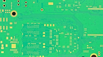
 Image 2: PCB Tinning
Special Offer: Get $100 off your order!
Email [email protected] to get started!
3、What PCB Tinning Solutions are Made of
The Tinning solution is made up of many materials. Some of these materials are everyday items that can be bought locally.
Some of these materials must be purchased from merchants specializing in PCB and tinning materials.
While not all these materials are necessary to make a tinning solution, select materials are needed.
Because so many variables go into a tinning solution, there are many different ways to create PCB tinning from chosen materials.
3.1 Thiourea - The essential ingredient for PCB tinning
The tin plating solution is made of the silver polishing agent, commonly used to clean jewelry.
Many do not know that silver polish contains Thiourea, the most necessary agent for creating a tinning solution.
Thiourea is combined with other materials to create a tinning solution.
Making a tinning solution from scratch is impossible without extracting the Thiourea from silver polish.
Thiourea is so active on its own as a compound that it can create electroless tin plates with it that do not require a charge to conduct electricity.
Since silver polish can be bought from a typical store, it is possible to create any tin plating with everyday items.
However, not every tin plate is designed the same, and to make things even more complicated, each has different functions.
3.2 Other ingredients that will assist in creating a tinning solution
While Thiourea is necessary to create a tinning solution, other materials will make creating a tinning solution a much easier process.
The first of these is hydrochloric acid, also known as muriatic acid.
Although this cannot be purchased directly as a silver polishing can, it can be made from household items.
Solid, lead-free solder is the second ingredient that can combine with silver polish to create a tinning solution.
Soldering liquid is another thing that is essential to creating a tinning solution and crucial to designing printed circuit boards in and of themselves.
3.3 Create the skills needed for tin plating solutions
Creating tin plating solutions, especially when using household items from scratch, will require some skills.
Many "experts" in PCB-related issues will foolishly say that it is easy to ultimately make tinning solutions and printed circuit boards with household items.
It is possible, and these individuals are not wrong.
However, making your printed circuit board and tinning solution does require specific skills and knowledge.
Moreover, while these skills can be learned from tutorials, there is a significant risk to this.
The one skill that will make you a much longer way to create a tinning solution and other materials related to printed circuit boards is introductory chemistry.
The materials above and compounds are all compounds that require at least a basic understanding of the numbers and formulas that entail the discipline of chemistry.
It does not require a college degree to master introductory chemistry.
Like with most DIY guides, a person can google their way to acquire this knowledge.
Most materials mentioned above have all the information needed to mix correctly.
Learning the basics of chemistry to start creating your printed circuit boards and tinning solutions without outside help is possible.
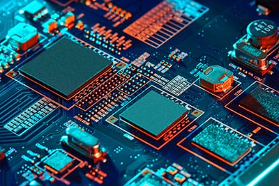
 Image 3: PCB Tinning
4、DIY PCB Tinning
All of the above information points out that DIY PCB tinning is not only possible but also difficult to do if you possess the right materials and skills.
That being said, there are many precautions to take if you create your PCB tinning solution and apply PCB tinning to your own homemade printed circuit boards.
Since DIY PCB tinning involves household items, it can also cost some money. This chapter will cover both of these.
 Image 4: PCB Tinning
4.1 Things to watch out for
The stereotype of fluids being placed into tubes and blowing up in chemistry classes is not entirely wrong.
Do not forget that printed circuit boards revolve around electric charges and generating power to and from a source.
Moreover, although PCB tinning is done when a printed circuit board is not necessarily active, dangers are still involved.
As you can see from the above picture, not only does the creation of almost anything related to a printed circuit board involve many small materials, but these materials are very fragile and under much pressure.
Take tin plating chemicals such as Thiourea, for example.
While it will not necessarily combust when mixed, it can still contaminate food and fluids around it, and it can make these things toxic when other people unaware of it come in contact with it.
It is made explicitly clear in this instructional guide for anybody interested in electroless tin plating.
Another precaution to be taken when it comes to PCB tinning is heating.
While using electrical components or heat to solder tin into a printed circuit board is unnecessary, heating will speed up the tinning process, as revealed in this other guide.
Anything involving intense heat, which is the case for soldering, needs to be micromanaged because of the unpredictability of heat when it comes to its surroundings.
Be aware of your surroundings if you have decided on a solder tinning solution to apply to a printed circuit board.
 Image 5: PCB Tinning
4.2 How Much Does it Cost to Do DIY PCB Tinning?
Another thing to consider when it comes to DIY PCB tinning is how much it costs to gather the materials and where to get them.
As you can see from the picture above, many materials go into creating a printed circuit board, and PCB tinning is no exception.
Silver polish, broken down into Thiourea, can be bought online for roughly $10.
In its natural solution state, Thiourea can be purchased for a little over $50.
The problem with silver polish is that it needs to break down with specific materials that produce the right amount of heat and pressure.
It must also be combined with other compounds to break down properly.
The price of these materials will vary, but if you are dedicated to doing PCB tinning out of your own home, prepare to spend over $100 on all necessary supplies.
If you want to create an entire printed circuit board, you will likely need to pay $500 for the materials, including the copper and tin components.
 Image 6: PCB Tinning
5、Is PCB Tinning Necessary?
Recall that the entire purpose of PCB tinning is to prevent the copper materials in a printed circuit board from encountering corrosion if it is exposed to anything.
Consider that any printed circuit board will be exposed to outside elements.
PCB tinning will reduce the pressure from these external elements and impede the copper inside the circuit board from oxidizing, if not halt it outright.
Some argue that PCB tinning is optional, and they would be correct.
It is never a requirement for any given printed circuit board to be tinned.
After all, it would operate the same without tinning as otherwise. The question, therefore, is one of longevity.
When a printed circuit board is tinned, it guarantees that the copper inside it will last much longer.
Additionally, PCB tinning will naturally enhance the current in the tracks of the circuit board and will allow it to operate and perform much more consistently.
A printed circuit board without tinning can be compared to a house with an old, unstable roof.
While the top will still protect from outside forces, it would not be nearly as effective as a brand-new roof.
PCB tinning will provide a "new roof" for the copper tracing inside a circuit board.
6、Conclusion
Many materials go into a printed circuit board.
It takes a lot of time and effort to gather these materials and create a printed circuit board that will work effectively.
One final thing that needs to be understood is that very little guesswork is allowed in constructing a printed circuit board.
PCB tinning is seen as an inconvenience for some, as anybody who has decided to create a printed circuit board from scratch should understand that the efficiency of their printed circuit board will be enhanced to much higher levels if they choose to do PCB tinning.
Also, the best thing about PCB tinning is that it can start from scratch, mainly household items.
DIY PCB tinning is quickly done by learning a few skills and putting forth time and money to gather the right supplies.
Special Offer: Get $100 off your order!
Email [email protected] to get started!