Even as systems and computing power advance, it is still impossible to control electric pulses because power flows as an analog waveform. Therefore, it is necessary to develop safeguards to handle power spikes so that they don't damage system components. One such safeguard is the snubber circuit, which usually consists of a simple resistor-capacitor or resistor-capacitor-diode design. We have covered the protective circuit below, including its analysis, design, and applications. Take a look!
Contents
- What is a Snubber Circuit?
- General Classifications of Snubber
- Lossy or Dissipative
- Non-lossy or Non-dissipative
- Lossy and Non-lossy Snubber Power Loss Comparison
- Commonly Used Snubbers in Practical Applications
- RC Snubber
- Some RC Snubber Circuits
- RCD Snubber
- Some RCD Snubber Circuits
- Snubber Diode
- Snubber Circuit Design
- Methodology of Snubber Circuit Analysis
- Quantizing the Transient
- Frequency Response
- Snubber Circuit Parameters
- Summary
What is a Snubber Circuit?
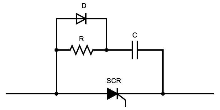
A snubber circuit is a resistor and capacitor connected across a thyristor in its simplest form. Its purpose is to protect the electrical components from transient voltage spikes or enhance performance.
A trial snubber circuit
Source: Wikimedia Commons
The circuit is common in semiconductor devices and is capable of doing several functions, including the following:
- Damping voltage to reduce EMI
- Minimizing total switching losses
- Limiting dV/dt or dl/DT
- Minimizing or eliminating a current or voltage spike, or both
- Shaping the load line to maintain it in the safe operating area
- Moving power dissipation from the switch to useful load or resistor
The circuit acts like Transient Voltage Suppressors (TVS), minimizing power dissipation in electronic switching networks.
A Transient Voltage Suppressor
Source: Wikimedia Commons
General Classifications of Snubber
The following are the two general classifications of snubber circuits.
Lossy or Dissipative
A lossy or dissipative snubber circuit draws power from the device. It is easy to design because it requires only a simple diode and a resistor as the dissipating elements. However, it is not energy efficient and not ideal for power supplies that need high efficiency.
Non-lossy or Non-dissipative
As the name suggests, this circuit is the opposite of the lossy/ dissipative type. It is super-efficient and consists of inductors and capacitors. However, it is complex to design and expensive to build.
Lossy and Non-lossy Snubber Power Loss Comparison
The power losses in a dissipative circuit depend on the snubber device's selection. This device selection depends on the suppression level required for the transient voltage spike and ringing frequency. In most cases, the snubber losses are low and tolerable, so circuit designers use this type for quick & easy designs.
On the other hand, non-lossy snubber circuits are ideally lossless on paper, but this is not what happens practically. There are some minor losses, but they are negligible compared to the power flowing from the power supply line. For instance, the loss might be less than 1W for a 500W power supply line, representing less than 0.2%.
Special Offer: Get $100 off your order!
Email [email protected] to get started!
Commonly Used Snubbers in Practical Applications
There are many snubber variations, but the designs usually concentrate on the following three primary configurations.
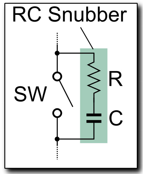
RC Snubber
An RC snubber is the most common of the three, and it consists of a resistor-capacitor (RC) duo joined in series. It applies to both the damping & rising control, and a well-designed circuit can control DC or AC loads. This snubber circuit is ideal for inductive loads, such as electric motors.
To function effectively, the resistors in the circuit must have a low inductance to prevent excessive ringing or overshoots. On the other hand, the capacitors should have a reduced series inductance to prevent unwanted resonance in the circuit.
Some RC Snubber Circuits
Buck Converter
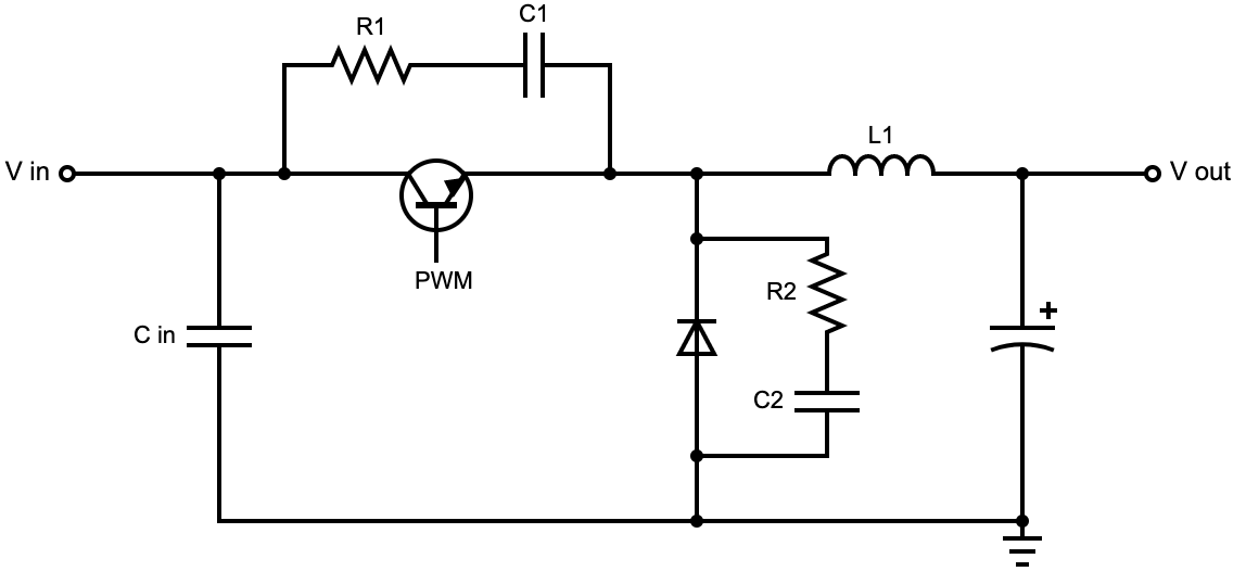
A buck converter circuit diagram
R1 and C1 form the first snubber-resistor snubber-capacitor circuit, while R2 and C2 form the second circuit.
DCDC Synchronous Rectifier

A DCDC synchronous rectifier circuit diagram, Note the two snubber circuits.
Boost Converter Topology
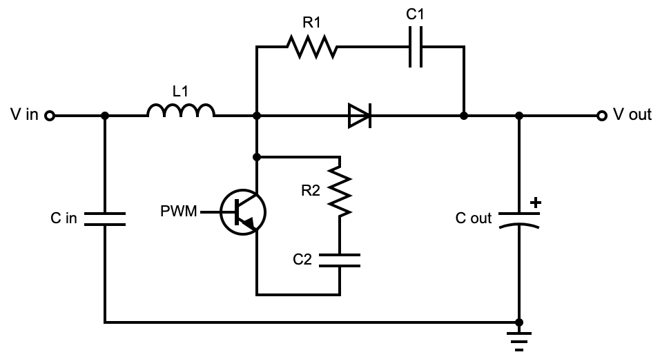
A circuit diagram for a boost converter topology, Note the two snubber circuits.
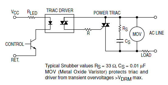
RCD Snubber
An RCD snubber contains three external components: a resistor, capacitor, and diode, hence RCD. The design is applicable for clamping voltage transients because the clamping presence of the diode in the circuit makes it a polarized snubber. While doing so, the RCD circuit does not alter the spike or the ringing frequency.
MOSFET drain turn-offs usually use this configuration, but the capacitor must get charged fully or discharged during each cycle.
Some RCD Snubber Circuits
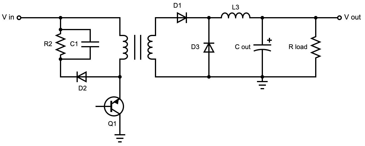
Flyback Converter

A flyback converter circuit diagram
R2, C1, and D2 form the RCD snubber circuit.
Forward Converter
A forward converter circuit diagram. Note the snubber circuit.
Snubber Diode
Also called a flyback or freewheeling diode, a diode snubber is a simple diode used to eliminate the sudden rise in voltage. This spike is the one that is noticeable across an inductive load when the input voltage reduces or does off suddenly.
Snubber Circuit Design
As explained earlier, a snubber circuit primarily consists of a resistor-capacitor combination connected in series. The resistor-capacitor (RC) snubber then connects to a thyristor in parallel. When the device voltage goes through, the circuit behaves like a short circuit at first because it reduces the output voltage to nil.
A snubber circuit design diagram
But the capacitor voltage gradually increases at a slow rate as it charges, ensuring the rate of voltage range (dv/dt) going through the thyristor is within range. Before turning on the thyristor, the capacitor must get fully charged. The capacitor discharges smoothly after turning it on via the thyristor or SCR (Silicon-Controlled Rectifier).
As it discharges, the resistor limits the current of capacitor flow to maintain the value and di/dt (rate of change) within the safe boundary.
It is important to note that the circuit must meet two requirements due to its subjection to high peak currents and voltage changes (DV/DT). These are:
- The stored energy in the snubber capacitor must be higher than the inductance energy in the circuit
- The time constant of the snubber circuit should be 10% of the expected on time
Methodology of Snubber Circuit Analysis
A snubber circuit analysis consists of the following three primary steps.
Quantizing the Transient
This step involves studying, analyzing, and modeling the concerned area and the equipment connected downstream using Electromagnetic Transient Programs (EMTP). You can extract vital parameters like the frequency, rise rate, magnitude, and energy from the proposed simulations. These simulations include those of the worst-case scenario, such as when there is equipment failure.
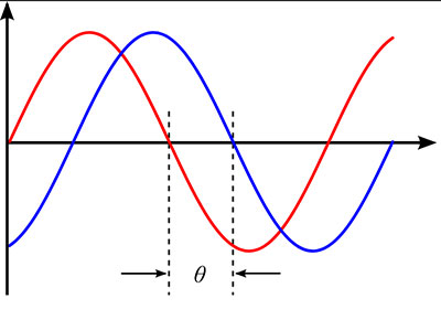
Frequency Response
The next step is frequency response analysis downstream of the faulty area to identify any occurrence of resonance between the system and transient frequency. This process occurs recursively at each point where a fault can occur to avoid an occurrence of a similar event.
RC Snubber Model
Source: Wikimedia Commons.
Snubber Circuit Parameters
The last step involves recommending suitable parameters for the snubber circuit's design to minimize power surges and switching transients to an acceptable or desired level. This recommendation is vital because it primarily helps to synchronize the frequency response of the system and the connected snubber circuit. While doing so, record the deviation for further analysis.
Summary
There you have it! A snubber circuit might be a simple addition to your circuit's board design, but it helps regulate the power supply from damaging critical electrical components inside. If you have questions about its design, analysis, etc., reach out for further information.
Special Offer: Get $100 off your order!
Email [email protected] to get started!