The 2020 to 2022 global integrated circuit shortage reminded us how important ICs are. They make mass production of modern electronic products possible. An important feature of current ICs is their packaging. Much like the circuit boards they attach to, they require a specialized substrate. Thus, we must understand why the substrate is a significant part of the integrated circuit’s structure. As such, this guide explores the IC substrate, how manufacturers produce and apply it, and the manufacturing technology involved in its creation. By the end of this guide, you’ll have everything you need to know about IC substrates, including how to get an accurate PCB quotation online for your projects.
Contents
- What is IC Substrate?
- Classifications of IC Substrate
- By Package Types
- By Bonding Technology
- By Material Characteristics
- Applications of IC Substrate PCB
- Characteristics of an IC Substrate
- Manufacturing Technology of IC Substrates
- Manufacturing Process of IC Substrate
- Manufacturing Difficulties of IC Substrate
- IC Substrate Manufacturing
- Microvia Manufacturing Technology
- Patterning and Copper Plating Technology
- Solder Mask
- Surface Finish
- Inspection Capability and Product Reliability Test Technology
- Composition of IC Packaging and Cost
- Conclusion
What is IC Substrate?
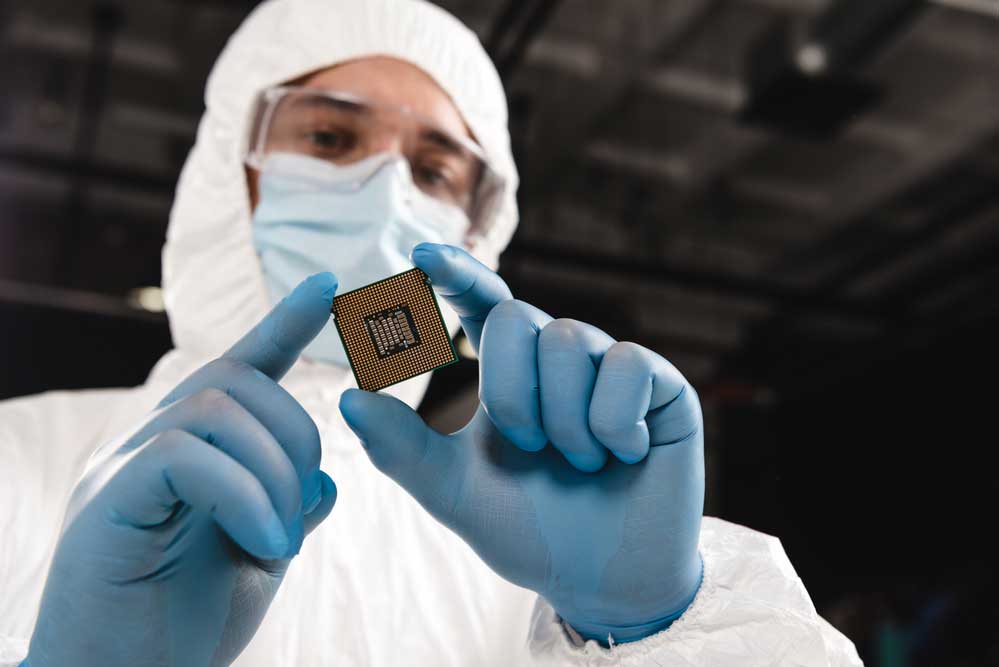 A worker holding an integrated circuit
The integrated circuit substrate (or IC package substrate) is the base material of IC packages. In addition to protecting the bare IC, they also facilitate connections between the IC and the PCB’s network of traces. As such, the substrate largely influences circuit performance.
They consist of several layers and a supporting core in the middle. Moreover, the IC substrate contains a network of drill holes and conductor pads. Often, these exceed the density of conventional PCBs. Thus, they can be pretty complex to fabricate.
Classifications of IC Substrate
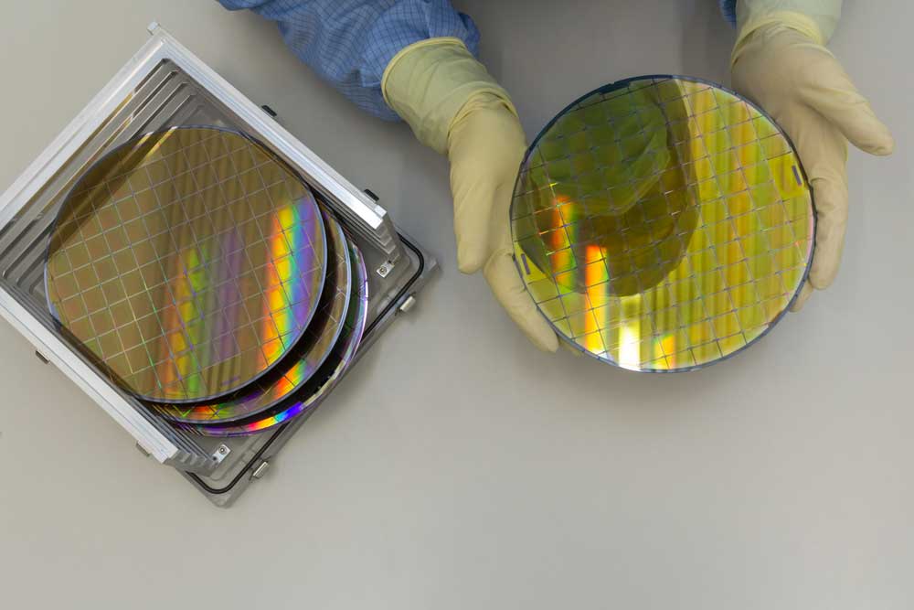
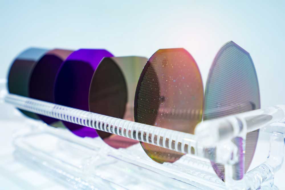 Silicon wafer for construction of Integrated Substrates
IC substrates are varied and fall under three main classifications. These classifications include the package/packaging type, bonding technology, and material attributes/characteristics. Additionally, we may divide them into application fields.
By Package Types
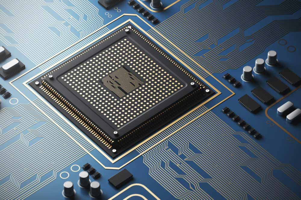 IC on blue circuit board
The package type describes the type of carrier. As such, each package may require a different variety of substrates.
- Ball Grid Array IC substrate: this type of substrate is suitable for IC packages with a large pin count (>300). Intrinsically, we can attribute this to its excellent electric performance and heat dissipation.
- Chip-scale package IC substrate: this type of substrate is miniaturized and thin. As such, it’s suitable for smaller single-chip packages with a small pin count (CSPs).
- Flip-chip IC substrate: this type of substrate is most appropriate for controlled collapse chip connections in a flip-chip chip-scale package (FCCSP). Thus, it has good heat dissipation protection against circuit loss and signals interference.
- Multi-chip module IC substrate: Substrates in this type of packaging hold multiple ICs. Each IC may have a different function. Consequently, the substrate must be lightweight. However, because of the nature of MCM ICs, this substrate may not have sound signal interference, good routing, or good heat dissipation.
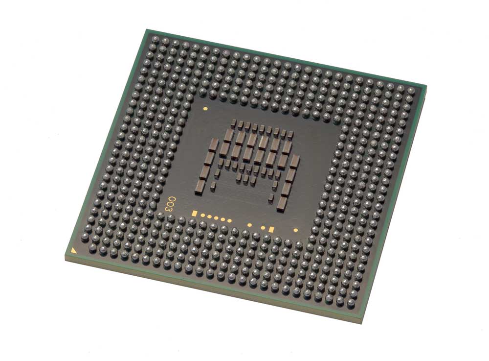 IC with solder ball grid array
By Bonding Technology
The bonding technology describes how the integrated circuit bonds to the package or external circuitry. Again, each bond may require a substrate with unique characteristics.
- Wire bonding: It is the most common type of bonding. Typically, an operator or machine will thread wires from the connections on the chip to the package/carrier or external circuit.
- Tape automated bonding (TAB): Describes the creation of flexible printed circuits (FPC) where manufacturers bond an integrated circuit to fine conductors in a polymer-based substrate.
- Flip Chip (FC): The most common way of facilitating interconnections in this type of bonding is by using solder balls/bumps. Next, after we disperse solder balls on the chip pads, we flip the chip over and align it to the external circuit’s pads. Incidentally, manufacturers can create this bond with either a polymer adhesive, welded joint, or solder interface.
By Material Characteristics
Since integrated circuits have different functions, their substrates will require different material types and characteristics. The most common are:
- Rigid: Manufacturers use resin to create these types of substrates. Consequently, they can either consist of Ajinomoto Build-up Film (ABF), Epoxy, or Bismaleimide Triazine (BT) material.
- Flex: We use Polyimide or Polyamide resin to manufacture this type of substrate. Incidentally, they both feature a similar electrical performance and coefficient of thermal expansion.
- Ceramic: We use ceramic material to create this type of substrate. Typically, it’s composed of either aluminum nitride, silicon carbide, or aluminum oxide.
Applications of IC Substrate PCB
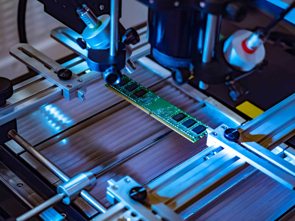 Installation of integrated circuits onto a RAM module
We can use IC substrates for:
- Memory chip packaging
- Packaging for micro-electromechanical systems (MEMS)
- Radiofrequency (RF) chip packages
- Packaging for processor chips
- Packaging for Integrated circuitry in high-speed communication devices
We can find these chips along with their packaging (that IC substrates make possible) in real-world applications such as
- Mobile smart devices such as smartphones and tablets
- Laptops, printers, and memory products (such as RAM modules)
- Medical devices
- Telecommunications
- Aerospace & military
- Industrial machinery
Special Offer: Get $100 off your order!
Email [email protected] to get started!
Characteristics of an IC Substrate
 A worker holding silicon wafers
Integrated Circuit substrates feature a diverse set of attributes and characteristics. Some of them include:
- Lightweight: IC Substrates are generally light. This is mainly due to the material they use.
- Extremely reliable: These substrates form a protective layer around the integrated circuit. As such, they must consist of solid material.
- Require fewer wires and solder joints: IC substrates are generally smaller than typical PCB substrates. Thus, they require fewer wires and solder joints.
- Compact: IC substrates sport a miniaturized design. Consequently, they require fewer materials to construct.
- Durable: Despite their size, IC substrates are robust.
Manufacturing Technology of IC Substrates
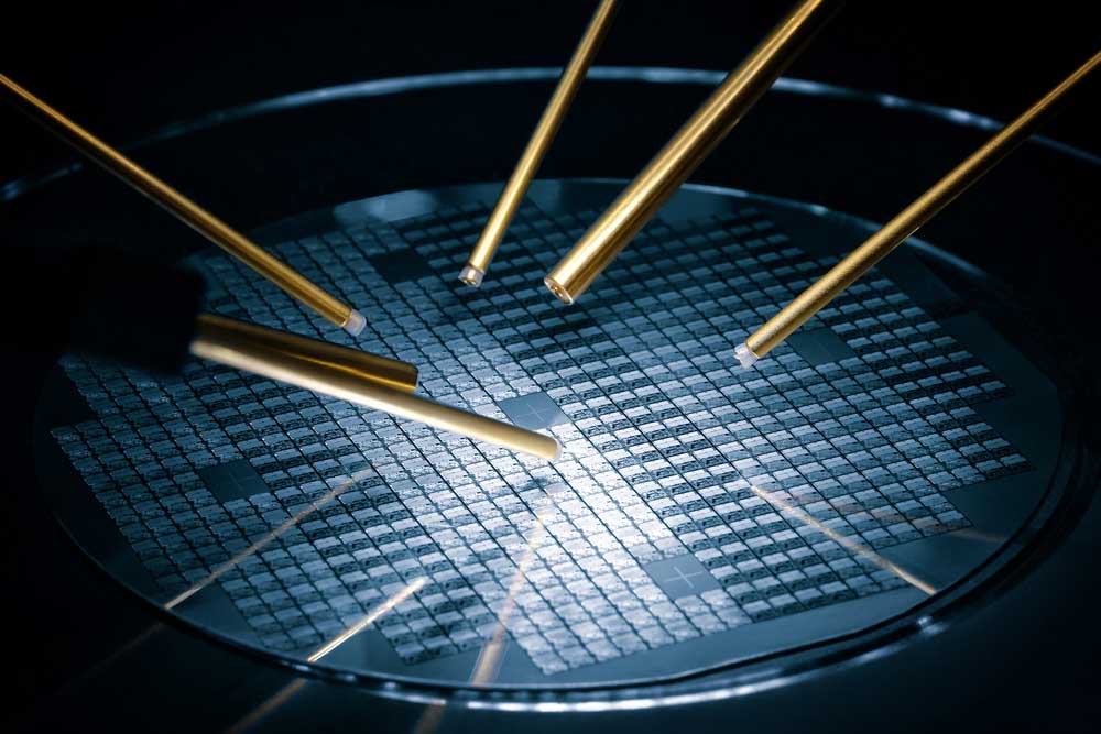
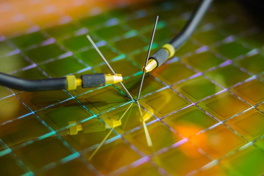 Machine probing microchips on a silicon wafer
There are three types of manufacturing methods for IC substrates. They include:
- The subtraction method (SP) is the most common IC and PCB manufacturing method. It involves first applying a copper layer on a copper-clad laminate. Next, the substrate manufacturer uses a dry film coating to protect the circuits and thru-holes. Lastly, the manufacturer will then etch off any unnecessary copper sheeting.
- Addition Method (AP): The manufacturer will apply an insulating substrate to an exposed circuit. Incidentally, the insulating substrate will contain a photosensitive catalyst. Next, the manufacturer will selectively deposit a stream of a chemical copper compound on the course.
- Modified semi-additive process (MSAP): The method will electroplate the thin copper layer on the main laminate. Next, the manufacturer will apply a protective layer on the areas of the laminate where electroplating isn’t possible or necessary. The manufacturer then electroplates the laminate and coats the substrate with an anti-corrosive chemical. Next, the manufacturer refines the substrate by removing excess copper through a flash etching process.
Manufacturing Process of IC Substrate
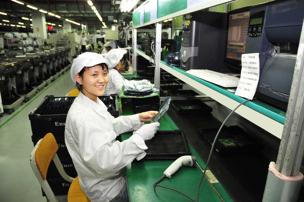
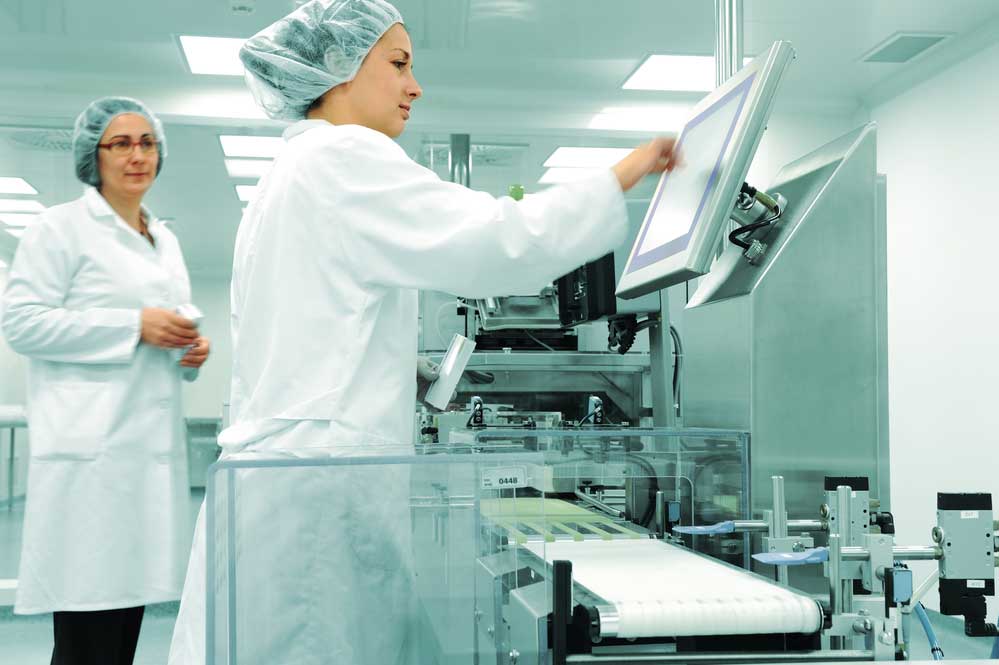 Female operators at a production line in a manufacturing plant
- Copper patterning and plating: This involves preparing the copper material by manipulating and shaping it. As such, this technique requires machinery that adjusts the thickness and shape of the copper. Consequently, it’s the first step in the manufacturing process.
- Solder Mask: This involves applying a solder mask to the substrate. The substrate manufacturer will use a combination of solder mask printing technology and equipment for through-hole filling.
- Surface finishing: This process involves buffing and polishing the substrate to ensure that it has a uniform and even surface.
- Inspection: The manufacturer must test the final substrate for integrity and reliability during this process.
Manufacturing Difficulties of IC Substrate
Because the IC substrate fabrication process can be pretty complicated, it comes with many challenges. Consequently, some of these difficulties include:
IC Substrate Manufacturing
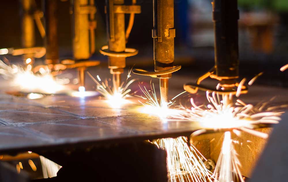 Up close Image of CNC LPG cutting
Because of the size and consistency of IC substrates, they can be pretty fragile and easy to distort. Furthermore, this fact is especially actual for substrates with less than 0.2mm width. We can control and prevent deformities in the substrate by providing improved lamination parameters and layer positioning. Moreover, we need to pay careful attention to the plate shrinkage process for maximum performance.
Microvia Manufacturing Technology
This technology involves applying laser-drilled and plated through-holes, conformal masks, and copper plate filling. Again, applying this technology can be tricky because of the miniaturized scale of most integrated circuits and their substrates. However, we can use blind and conformal masks to make laser drilling easier.
Patterning and Copper Plating Technology
External patterning can be complex, especially for smaller form factors. The technology features circuit control and compensation equipment, industrial control for uniform copper plating thickness, and thin wire manufacturing. These technologies are also involved in bonding.
Solder Mask
 A substrate with solder joints and solder masks
Creating a solder mask is essential for the IC substrate manufacturing process. As such, the surface of the IC substrate generally does not exceed 10um. Furthermore, the size difference between the solder mask and pad must not be greater than 15 microns. Thus, applying the solder mask for IC substrates requires more care than PCBs. Accordingly, we must use specialized technology, equipment, and procedures for solder mask printing and through-hole filling.
Surface Finish
 Worker checking an integrated circuit board in a factory
Surface finishing involves buffing and smoothing the IC substrate. It may not be as complex as the other steps in the manufacturing process but still requires special care. Consequently, we must focus on ensuring the surface of the IC substrate is uniform. Typically, manufacturers use either electroless nickel immersion gold (ENIG) or nickel electroless palladium immersion gold (ENEPIG) for the surface finish.
Inspection Capability and Product Reliability Test Technology
 A test sample of a miniaturized integrated circuit under a microscope
The final phase of the manufacturing process. Notably, manufacturers require different inspection techniques and technology to test and ensure the wholeness of the complete IC substrate. Furthermore, it requires experienced operators and technicians familiar with these techniques and technology.
Composition of IC Packaging and Cost
The substrate is the main component of the packaging. Thus, depending on its material, it’s the most expensive aspect. Again, the substrate can be rigid (hard), soft/flexible, or ceramic. Ceramic substrates tend to take longer to produce. Contrastingly, flexible and rigid substrates tend to take a similar amount of time to create.
Another critical aspect of the IC packaging is the ultra-thin electrolytic copper foil. The IC substrate requires it to be completely uniform with a density of 1.5μm. Incidentally, the price of ultra-thin electrolytic copper foil is greater than that of its regular counterpart.
Conclusion
The above guide explores all the aspects of integrated circuit substrates. They have many similarities to PCB substrates. However, they are more specialized because of their size. Additionally, IC substrates and their materials are slightly more diverse.
Nevertheless, the production of IC and PCB substrates requires an experienced manufacturer. For instance, an industry leader can source the best materials and utilize the latest technology to produce high-quality circuit boards. From Gerber design validations to accurate inspection of the finished product, OurPCB is the obvious choice for a high production yield. Notwithstanding, we hope that you’ve found this guide to be helpful. Thank you for reading.
Back to top: IC Substrate
Special Offer: Get $100 off your order!
Email [email protected] to get started!