
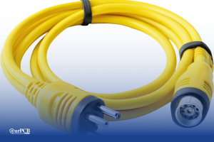
Top 7 Truck Wiring Harness Manufacturers
Truck wiring harnesses are the electrical backbone of commercial vehicles, from long-haul trucks to construction fleets and emergency vehicles. They must withstand continuous vibration, thermal

As a leading PTFE PCB manufacturer, OurPCB specializes in fabricating printed circuit boards that use PTFE substrates for high-frequency and RF applications. By working with PTFE laminates known for their low dielectric constant, thermal resistance, and minimal signal loss, our PCBs deliver reliable, high-speed performance in aerospace, medical, and communication systems.


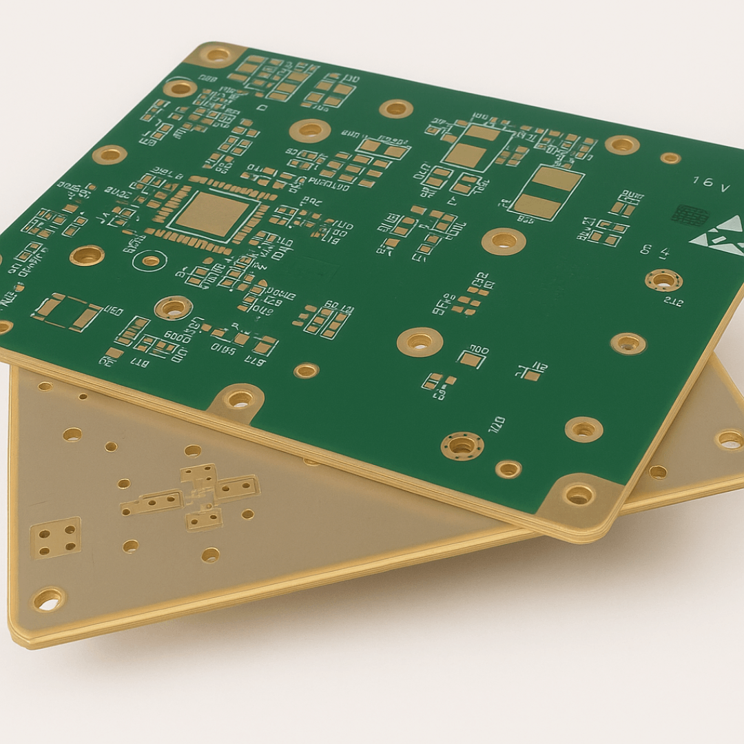

PTFE PCBs are printed circuit boards that use polytetrafluoroethylene (PTFE) as the primary dielectric substrate to support high-frequency, low-loss electrical performance. PTFE, commercially known under brand names like Teflon, provides a dielectric constant between 2.17 and 2.40 and a dissipation factor below 0.0015 at 10 GHz, making it one of the most stable materials for RF, microwave, and high-speed digital circuit fabrication.
Teflon PCBs minimize signal distortion and propagation delay by maintaining uniform electrical properties across a wide frequency and temperature range. Their extremely low moisture absorption rate, usually below 0.01%, protects against dielectric instability in humid environments, while high electrical surface resistivity exceeding 10¹³ ohms ensures excellent isolation between adjacent traces.
These characteristics make PTFE laminates ideal for circuits requiring controlled impedance, minimal signal attenuation, and stable phase characteristics over operational frequencies ranging from 1 to 77 GHz.
Manufacturing PTFE PCBs requires specialized techniques due to the material’s low surface energy, high thermal expansion coefficient, and mechanical softness. Processes such as plasma surface activation, slow-feed high-RPM drilling, and nitrogen-assisted soldering are employed to ensure reliable hole wall plating, trace geometry accuracy, and long-term mechanical integrity.
PTFE PCB manufacturing requires precise control of material processing to achieve consistent dielectric performance, mechanical stability, and minimal signal loss across high-frequency ranges.
PTFE laminates, such as Rogers 5880 and 4350B, feature a low dielectric constant (around 2.2) and low loss tangent (under 0.0012 at 10 GHz), which allows circuits to maintain signal integrity even at microwave and millimeter-wave frequencies.
Working with PTFE substrates poses specific fabrication challenges due to their high thermal expansion and poor adhesion to copper, which makes drilling, hole wall plating, and multilayer lamination more complex than FR4-based PCB materials.
Specialized techniques, including slow-feed drilling to prevent material smearing, plasma treatment to improve resin adhesion, and precision-controlled reflow soldering under a nitrogen atmosphere, are used to ensure structural reliability and maintain electrical properties during PCB manufacturing and assembly.
Thermal management is important in PTFE circuit boards, as the coefficient of thermal expansion (CTE) for pure PTFE can reach 200 ppm/°C, compared to 14–17 ppm/°C for copper layers. Without proper compensation, CTE mismatches can lead to via cracking, delamination, and mechanical stress failures during thermal cycling.
Careful material selection, laminate bonding optimization, and reinforcement techniques such as woven glass reinforcement are employed to reduce expansion and stabilize multilayer PCB structures for RF, aerospace, and medical electronic devices.


PTFE PCBs are widely used in aerospace and satellite systems, where circuits must maintain stable impedance and low signal loss across frequencies between 1 and 40 GHz.
PTFE laminates with dielectric constants around 2.17 to 2.40 and loss tangents below 0.0015 ensure minimal phase distortion and stable signal propagation in high-altitude, thermally variable environments.
Operating temperatures from -55 °C to +150 °C allow PTFE circuit boards to withstand rapid thermal cycling without delamination or performance degradation.
RF and microwave systems operating from 2 GHz to 77 GHz depend on PTFE PCBs for precise impedance control and low dielectric loss.
PTFE substrates offer dissipation factors as low as 0.0009 at 10 GHz, enabling low reflection coefficients and reduced insertion loss in antennas, amplifiers, and transmission line designs.
Those working with RF modules or phased-array radar benefit from PTFE’s stable dielectric constant across wide frequency and temperature variations, preserving signal quality in mission-critical environments.
Medical imaging equipment, including MRI and ultrasound systems, use Teflon PCBs to maintain signal integrity in low-noise, high-frequency circuits.
Laminates designed for dielectric constants near 2.2 and extremely low loss tangents support clear signal paths with minimal electromagnetic interference, improving image resolution and diagnostic reliability.
PTFE circuit boards also resist moisture absorption and chemical degradation, preserving material stability inside sterilized or humid clinical environments.
Industrial sensors in sectors such as oil and gas, manufacturing automation, and environmental monitoring rely on PTFE PCBs for high-frequency signal processing and mechanical reliability.
PTFE laminates maintain stable electrical properties under exposure to vibration, corrosive chemicals, and wide temperature swings.
Glass-reinforced PTFE substrates reduce the coefficient of thermal expansion (CTE) below 50 ppm/°C, preventing micro-cracking of vias and solder joints under thermal stress.
Automotive radar systems and ADAS technologies depend on PTFE PCBs to handle frequencies between 24 and 77 GHz for object detection, collision avoidance, and lane tracking.
PTFE materials minimize signal loss and phase variation even as ambient vehicle temperatures fluctuate between -40 °C and +125 °C.
Low-loss PTFE laminates, such as Rogers RO3003 and RO4350B, provide the necessary dielectric stability and mechanical endurance required in safety-critical automotive applications.
High-frequency testing platforms, including network analyzers and signal generators, incorporate PTFE PCBs to maintain low signal distortion and accurate measurement across the 1 to 50 GHz range.
Circuits fabricated on PTFE materials with tightly controlled dielectric constants and minimal loss tangents reduce measurement uncertainty and preserve system calibration over time.
Engineers designing test equipment rely on Teflon circuit boards to achieve stable performance even under rapid signal switching and thermal cycling.

PTFE PCBs maintain a dielectric constant between 2.17 and 2.40, allowing consistent signal velocity and impedance control across frequencies from 1 to 77 GHz.
This stability reduces phase distortion and supports tight trace impedance matching, making PTFE laminates the preferred substrate for RF, microwave, and high-speed digital circuits. This helps maintain signal integrity across operating temperatures and wide bandwidths.
The dissipation factor of PTFE PCB materials remains below 0.0015 at 10 GHz, significantly lowering signal attenuation over transmission paths.
This low loss tangent directly improves insertion loss performance in radar modules, satellite communication systems, and high-frequency amplifiers.
PTFE substrates can extend circuit operating ranges without the need for additional amplification or complex signal conditioning stages.
PTFE laminates are available in pure PTFE and glass-reinforced PTFE variants, each offering specific mechanical and electrical performance characteristics.
Pure PTFE provides the lowest dielectric loss but has a higher coefficient of thermal expansion (up to 200 ppm/°C), while glass-reinforced PTFE reduces CTE to around 50–70 ppm/°C, improving dimensional stability during thermal cycling.
Material selection depends on whether the application demands extreme RF performance or structural rigidity for multilayer PCB fabrication.
PTFE laminates exhibit moisture absorption rates below 0.01%, which protects circuit electrical properties from humidity-induced variability.
This feature ensures that RF signal transmission, dielectric constant stability, and impedance matching remain unaffected even in high-humidity environments such as aerospace cabins, outdoor communication towers, and industrial sensor networks.
Thermal conductivity values for PTFE PCB materials range from 0.25 W/m·K to 0.45 W/m·K, depending on filler content and reinforcement type.
While PTFE is not a high thermal conductor compared to ceramics, its predictable heat distribution supports steady-state temperature control in RF amplifiers, power dividers, and microwave transmitters.
Engineers working on high-power designs must account for thermal management strategies using these conductivity properties.
PTFE laminates provide electrical surface resistivity values exceeding 10¹³ ohms, offering strong isolation between adjacent conductors even at high voltages and frequencies.
This high resistivity reduces leakage currents, minimizes crosstalk, and preserves the signal integrity of sensitive RF and high-speed digital circuits operating in densely routed PCB layouts.
| Property | PTFE Laminates | FR-4 Substrates | Ceramic Substrates (e.g., LTCC) |
|---|---|---|---|
| Dielectric Constant (Dk) | 2.17 to 2.40 | 4.2 to 4.8 | 6.0 to 10.0 |
| Loss Tangent (Df) | 0.0009 to 0.0015 | 0.02 to 0.035 | 0.001 to 0.003 |
| Moisture Absorption | <0.01% | 0.10 to 0.25% | <0.01% |
| Thermal Conductivity (W/m·K) | 0.25 to 0.45 | 0.25 | 2.5 to 6.0 |
| Coefficient of Thermal Expansion (CTE) | 50–200 ppm/°C (depending on reinforcement) | ~70 ppm/°C | 5 to 10 ppm/°C |
| Frequency Range Suitability | 1 to 77 GHz | Up to ~5 GHz | Up to 100 GHz+ |
| Manufacturing Complexity | High | Moderate | Very High |
| Cost | High | Low | Very High |
OurPCB sources premium PTFE laminates and related materials exclusively from globally recognized suppliers to ensure consistent electrical, thermal, and mechanical performance across all high-frequency PCB builds.
Rogers Corporation provides widely used Teflon substrates such as RO3003, RO4350B, and RO5880, known for low dielectric constants (2.17 to 3.48), low loss tangents (0.0009 to 0.0037 at 10 GHz), and stable high-frequency characteristics. In addition to Roger’s Teflon PCB substrate, we also source PTFE laminates from other industry leaders, including Taconic, Isola, and Arlon.
PTFE PCB drilling requires spindle speeds between 180,000 and 250,000 RPM and feed rates of 20 to 60 micrometers per revolution to avoid material smearing and burring.
We use specialized drill bits with reduced point angles and optimized chip loads to manage PTFE’s soft, elastic properties. Plasma surface activation with argon gas follows drilling to improve copper adhesion inside hole walls, reducing the risk of via failure during thermal cycling.
OurPCB conducts multilayer lamination of PTFE PCBs under press temperatures ranging from 260 °C to 290 °C and pressures between 200 and 400 psi, depending on the laminate system used.
Stackup designs incorporate glass-reinforced PTFE prepregs when necessary to limit z-axis expansion and improve mechanical stability. Vacuum-assisted lamination is applied to eliminate voids and resin void formation, preserving dielectric uniformity for controlled impedance layers.
Due to PTFE’s higher etch rate compared to standard FR4, OurPCB uses shortened etchback timing and fine-line imaging adjustments to prevent over-etching of signal traces.
Copper thickness is measured and monitored before and after etching to maintain impedance targets within ±5% tolerance. Strict control over trace geometry is important to achieving high-frequency PCB performance in RF, microwave, and millimeter-wave bands.
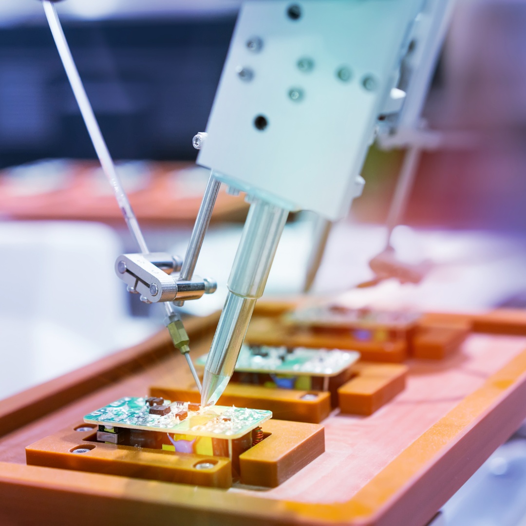
Soldering processes for PTFE PCBs involve nitrogen-purged reflow ovens to minimize oxide formation and enhance solder joint quality. Nitrogen environments allow lower peak soldering temperatures and improve solder wetting on PTFE surfaces treated with plasma activation.
This method strengthens joint integrity, reduces solder voids, and supports consistent RF signal transmission through high-reliability interconnects.
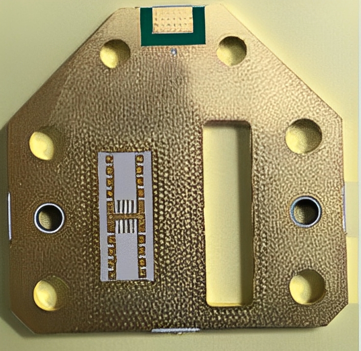
Microvia creation on PTFE laminates is managed through laser ablation using CO₂ or UV laser systems with pulse energy modulation to prevent thermal damage. Adjustments in laser parameters are made based on laminate filler type and reinforcement density to achieve clean via profiles without damaging the surrounding dielectric material.
Controlled laser drilling allows stacked, staggered, or blind/buried via structures critical for compact RF module designs.
PTFE PCB boards manufactured by OurPCB undergo automated optical inspection (AOI) and X-ray inspection for structural verification, followed by electrical testing for continuity, isolation, and impedance matching.
Time-domain reflectometry (TDR) analysis is used to measure transmission line impedance profiles across signal paths, verifying conformance to RF design specifications and ensuring signal integrity under operational frequencies up to 77 GHz.
PTFE PCB fabrication requires precise verification of electrical, mechanical, and thermal properties to maintain reliability in RF, microwave, and high-speed applications. OurPCB follows a structured testing and inspection workflow to meet international PCB quality standards, including IPC-6018 for high-frequency boards and IPC-A-610 Class 2 or Class 3 for finished assemblies.
During manufacturing, all PTFE PCBs undergo automated optical inspection (AOI) to identify trace width variations, opens, shorts, and registration defects. X-ray inspection is performed for multilayer assemblies and packages with hidden interconnects, such as ball grid arrays (BGAs) and stacked microvias. Electrical testing confirms netlist integrity, verifying continuity and isolation across all signal and power networks.
For high-frequency circuits, OurPCB applies time-domain reflectometry (TDR) testing to measure impedance profiles along transmission lines, checking that impedance stays within ±5% of target values. TDR results help engineers validate trace geometry, dielectric uniformity, and copper thickness against design expectations. In-circuit testing (ICT) is available for assemblies requiring functional validation of discrete components and system-level performance.
Testing records are archived with full material traceability documentation, providing customers with performance data linked directly to production batches. This testing approach ensures that PTFE PCBs delivered by OurPCB maintain consistent electrical performance, mechanical stability, and compliance with high-frequency design standards.
OurPCB sources premium PTFE laminates and related materials exclusively from globally recognized suppliers to ensure consistent electrical, thermal, and mechanical performance across all high-frequency PCB builds.
Rogers Corporation provides widely used Teflon substrates such as RO3003, RO4350B, and RO5880, known for low dielectric constants (2.17 to 3.48), low loss tangents (0.0009 to 0.0037 at 10 GHz), and stable high-frequency characteristics. In addition to Roger’s Teflon PCB substrate, we also source PTFE laminates from other industry leaders, including Taconic, Isola, and Arlon.
Our manufacturing operations span two facilities in Shijiazhuang and Shenzhen, totaling over 10,000 square meters of production space.
Factory infrastructure includes high-RPM drilling stations, laser drilling systems, nitrogen reflow ovens, automated optical inspection (AOI) lines, X-ray inspection stations, BGA rework platforms, in-circuit testing (ICT) systems, and plasma surface treatment chambers, all configured specifically for PTFE PCB processing and RF circuit fabrication.
Quoting processes at OurPCB deliver bare PCB estimates within 8 working hours and PCB assembly quotes with full component sourcing lists within 2 working days.
For time-sensitive RF or microwave projects, you can secure manufacturing slots and finalize procurement without extended negotiation or administrative delays, supporting tighter project schedules and accelerated prototyping cycles.
We use ROHS-compliant solder pastes, tin wires, and PTFE laminates across all production runs, ensuring that PCBs meet international environmental standards.
Our factories focus on reducing disposable material use, sorting and recycling production waste, and using energy-saving LED systems for manufacturing floor lighting. These practices align with customer requirements for both technical performance and environmental stewardship.
Decades of experience as a Teflon PCB manufacturer allow our technical teams to manage complex processing demands, including precise drilling parameter control, tight impedance matching, nitrogen-assisted reflow soldering, and multilayer lamination of low-loss substrates.
Integrated process monitoring ensures that mechanical, electrical, and thermal properties stay within specification, delivering consistent performance across RF, microwave, and high-speed digital circuit applications.
Mon-Fri: 24 hours,
Sat: 9am-6pm, GMT+8
Reach us at
[email protected]
24 hours online
+86-199-30589219
Mon-Fri: 24 hours,
Sat: 9am-6pm, GMT+8
Pure PTFE laminates offer the lowest dielectric constant and dissipation factor, making them ideal for extremely low-loss RF and microwave circuits. However, pure PTFE materials have high coefficients of thermal expansion (CTE) around 200 ppm/°C, which can cause dimensional instability in multilayer builds.
Reinforced PTFE laminates, which include woven glass or ceramic fillers, reduce CTE to 50–70 ppm/°C, improving mechanical stability while slightly increasing dielectric constant and insertion loss. Engineers select between pure and reinforced PTFE based on the trade-off between electrical performance and mechanical durability.
PTFE’s soft, elastic structure makes it challenging to drill clean holes without deformation. Specialized high-RPM drilling combined with slow feed rates and plasma treatment is required to prepare stable hole walls for plating.
Failure to control drilling parameters can lead to hole wall smearing, poor copper adhesion, and increased risk of via cracking during thermal cycling. To mitigate these risks, PTFE PCBs often incorporate modified resin systems or reinforced layers to stabilize mechanical behavior during via formation.
PTFE laminates exhibit relatively high thermal expansion compared to standard FR4 materials, with pure PTFE showing a CTE around 200 ppm/°C along the z-axis. This mismatch with copper layers can lead to mechanical stresses in vias and solder joints if improperly managed.
Glass-reinforced PTFE reduces CTE and helps balance expansion behavior, making it better suited for multilayer designs or circuits exposed to frequent thermal cycling between -55 °C and +150 °C.
Yes, PTFE PCBs can be fabricated as multilayer structures capable of supporting high frequency PCB signals. Multilayer PTFE stackups require careful lamination procedures using controlled temperature and pressure profiles to prevent resin squeeze-out and maintain uniform dielectric spacing.
Material selection often involves combining pure PTFE cores with reinforced PTFE prepregs to optimize electrical performance and mechanical integrity across multiple layers.
PTFE PCBs undergo comprehensive electrical and structural testing, including continuity and isolation verification, time-domain reflectometry (TDR) impedance analysis, and automated optical inspection (AOI).
For high-frequency applications, TDR results confirm that transmission line impedance stays within tight tolerance limits, while X-ray inspection detects hidden defects in solder joints, especially under BGAs or embedded RF modules.
These tests ensure that PTFE circuits meet RF performance and mechanical reliability requirements before final delivery.
We deliver PTFE PCB manufacturing services backed by certified processes, technical expertise, and complete material control for demanding RF, microwave, and high-speed circuit projects.
Truck wiring harnesses are the electrical backbone of commercial vehicles, from long-haul trucks to construction fleets and emergency vehicles. They must withstand continuous vibration, thermal

Medical cable assemblies sit at the intersection of electrical safety, biocompatibility, and sterilization durability. For regulated medical devices, OEMs must work with manufacturers that understand

Robotics cable assemblies are unlike ordinary cables, they must survive continuous motion, tight bend radii, torsion, vibration, electrical noise, and often harsh industrial or outdoor
Waterproof cable assemblies have to do more than just “keep water out.” For outdoor, marine, industrial washdown, and transportation platforms, assemblies are expected to survive
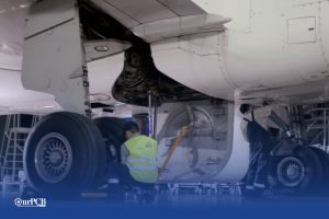
Aerospace cable assembly manufacturers work under standards such as AS9100, ISO 9001, and RTCA/DO-160, and many also maintain ITAR registration to support flight-critical and space-qualified

When considering the best places for manufacturing data cables, China immediately comes to mind. It’s no surprise either — the country has rapidly ascended in
We use cookies to improve your browsing experience, which may include personal information. By clicking "Agree," you accept our Privacy Policy and cookie use. You can change your cookie settings in your browser anytime.
Agree Chat With Us
 Free Quote