


End-to-End Production Control
We offer DFM review of your Gerber data, panelization strategy, controlled BOM handoff, and coordination of fabrication, assembly, test, and packing.
OurPCB project engineers schedule adherence, process quality, and cross-party communication, providing structured status updates from quotation through production release, in-process checkpoints, and final shipment.
Certified Quality Framework
PCB fabrication and assembly are executed under IPC-compliant workmanship criteria, such as IPC-A-610/IPC-601 within ISO-based quality systems. We also provide RoHS and REACH-compliant laminates, finishes, and components on request.
All our bare boards and critical components pass structured incoming inspection with lot-level traceability, including dimensional and solderability checks against IPC-6012 Class 2/3 and IPC J-STD-003 specifications.
Scalable Build Capacity for Mass Production
OurPCB supports the full product lifecycle, including the one-off and small-batch engineering builds for early hardware validation. We also cater to medium-volume pilot runs for certification, field trials, and market testing. Our build parameters are tuned at each stage to shorten iteration cycles without compromising manufacturability.
When products transition to high-volume mass production, we apply cost-optimized routing, material selection, and assembly processes under the same supplier umbrella, avoiding a disruptive vendor change.
Global Logistics, Export Compliance & Technical Support
Assemblies are packed in ESD-safe, export-ready configurations with moisture barrier protection, shock-resistant outer cartons, and clear labeling (part numbers, lot codes, HS codes) supported by complete commercial documentation for customs and compliance.
Our logistics team coordinates international air and sea freight under common Incoterms with established forwarders, while technical support engineers work daily with global hardware and purchasing teams to align on forecasts, shipment priorities, and issue resolution across time zones.

Our China-based turnkey PCB assembly demands tight integration between fabrication, component procurement, assembly, and testing. OurPCB operates this as one managed workflow so you can focus on your customers, rather than stress about your own capabilities.
Controlled Component Sourcing & BOM Engineering
We source active, passive, and electromechanical components primarily through authorized distributors and vetted regional suppliers. PCB assembly is bolstered using controlled AVL/AML lists and anti-counterfeit screening. BOMs are reviewed for lifecycle status, package compatibility, and RoHS/REACH compliance before purchase orders are placed, reducing the risk of last-minute substitutions and obsolescence surprises.
PCB Fabrication Options & Stackup Engineering
We support a wide range of laminate systems beyond standard FR-4, including high-Tg FR-4 for elevated thermal and mechanical stability, low-loss RF materials (e.g., Rogers-type), and hybrid stackups that combine multiple dielectrics for mixed-signal designs. Single-sided and double-sided boards can be built for cost-sensitive applications, while multilayer constructions support controlled impedance, dedicated reference planes, and high-current distribution across complex stackups.
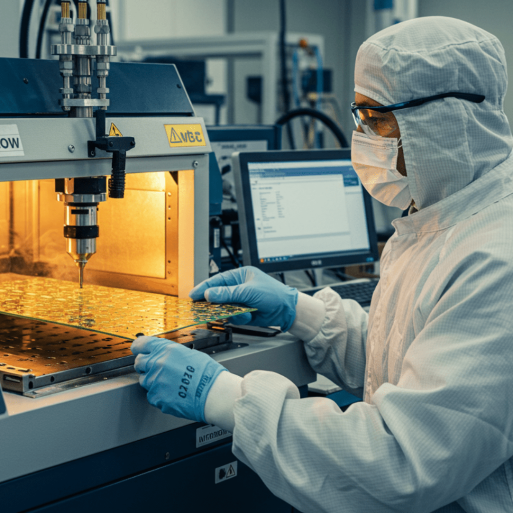
Our HDI capability includes laser-drilled microvias, blind/buried via structures, via-in-pad for fine-pitch BGAs, and sequential lamination to achieve higher routing density without sacrificing reliability. Surface finishes cover lead-free HASL, ENIG, ENEPIG, OSP, and other application-specific options, with copper thickness, soldermask registration, and impedance tolerances held to controlled specifications so signal integrity, assembly yield, and long-term reliability are maintained from prototype through volume production.
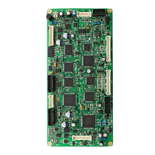
Assembly Capabilities & Process Controls
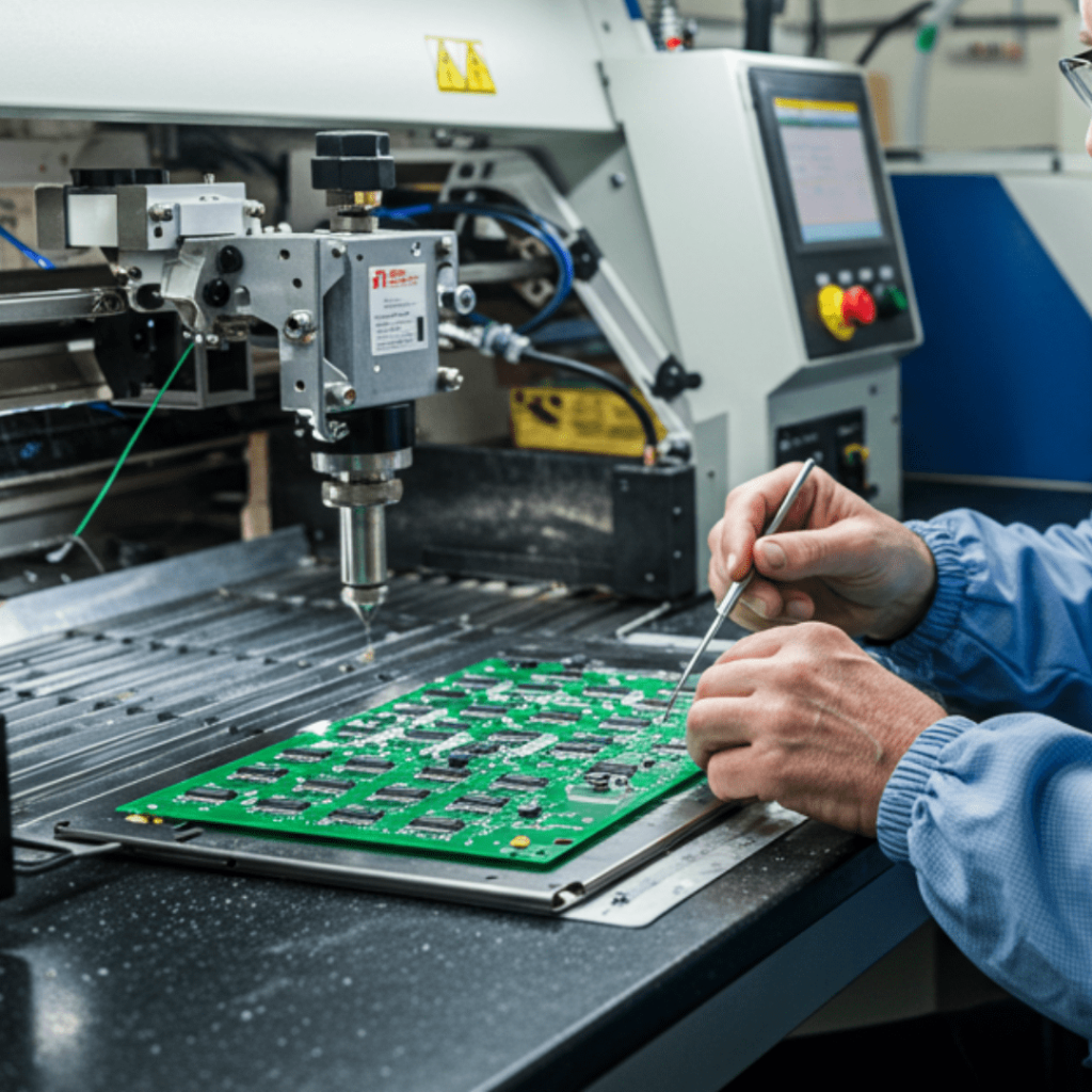
We run SMT, THT, and mixed-technology builds on automated lines with controlled solder paste printing (stencil design, alignment, and volume control), multi-zone reflow profiling, and inline SPI/AOI to maintain placement accuracy and wetting across fine-pitch and high-density designs. Fine-pitch QFPs, BGAs (including micro-BGA and CSP), and other area-array packages
Miniature passives down to 01005 and 0201 are supported with tuned pick-and-place libraries, feed mechanisms, and reflow profiles that account for tombstoning risk, thermal mass, and component skew on dense layouts. Mixed leaded and lead-free solder processes can be configured per project based on your requirements.
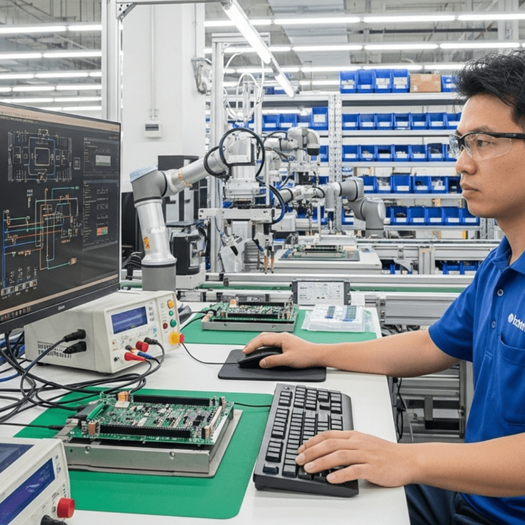
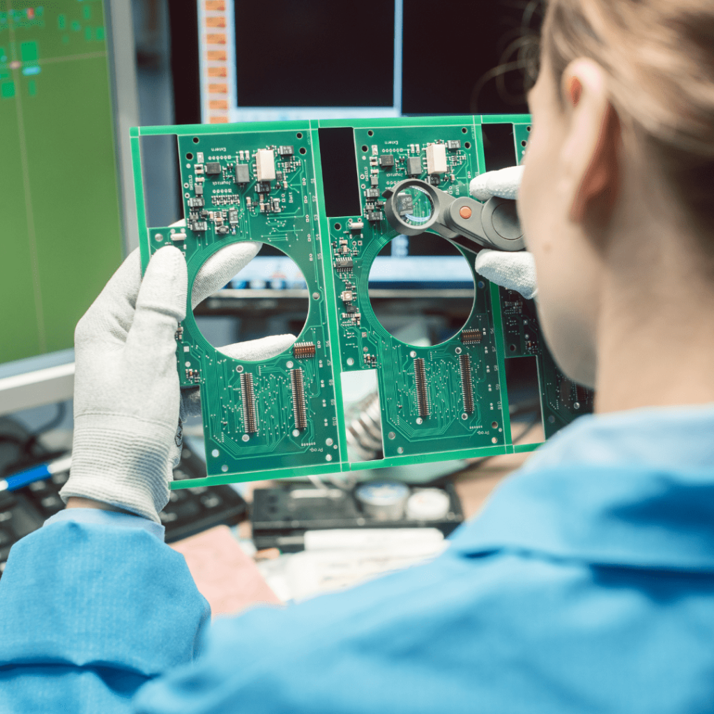
Testing, Inspection & Electrical Verification
SMT lines are equipped with inline SPI and AOI to verify paste volume, component presence, polarity, and solder fillet geometry, with inspection programs built directly from Gerber/CAD data and BOMs to maximize coverage on fine-pitch ICs and miniature passives. BGA, QFN, and other bottom-terminated packages are inspected using X-ray (2D/2.5D) to confirm
We support in-circuit test (ICT) using bed-of-nails to measure component values, continuity, and shorts, and functional test (FCT) built around customer test specifications, harnesses, and load conditions. Microcontrollers, FPGAs, and other programmable devices can be programmed and calibrated in-line or off-line via dedicated fixtures and programming adapters, with firmware revision, calibration constants, and serial IDs recorded as part of the test report and shipped.
Documentation, Traceability & Configuration Control
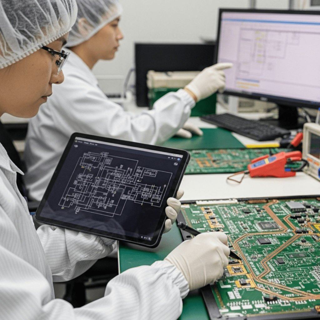
PCBs, components, and production batches are tracked at lot level through the full build path, with unique identifiers linking material receipts, process routes, inspection records, and shipment data to each work order. Traceability can be extended to serial-number level for assemblies where regulatory or customer requirements demand unit-level history.
Build packs include controlled documentation sets, including Gerber/CAD, BOM, pick-and-place, and test procedures. On request, we also supply structured test reports, AOI/X-ray summaries, and incoming/outgoing inspection records with recorded measurement data and defect logs, so quality events can be traced back quickly to specific lots, processes, or component sources.
Value-Added Services, Protection & Final Integration
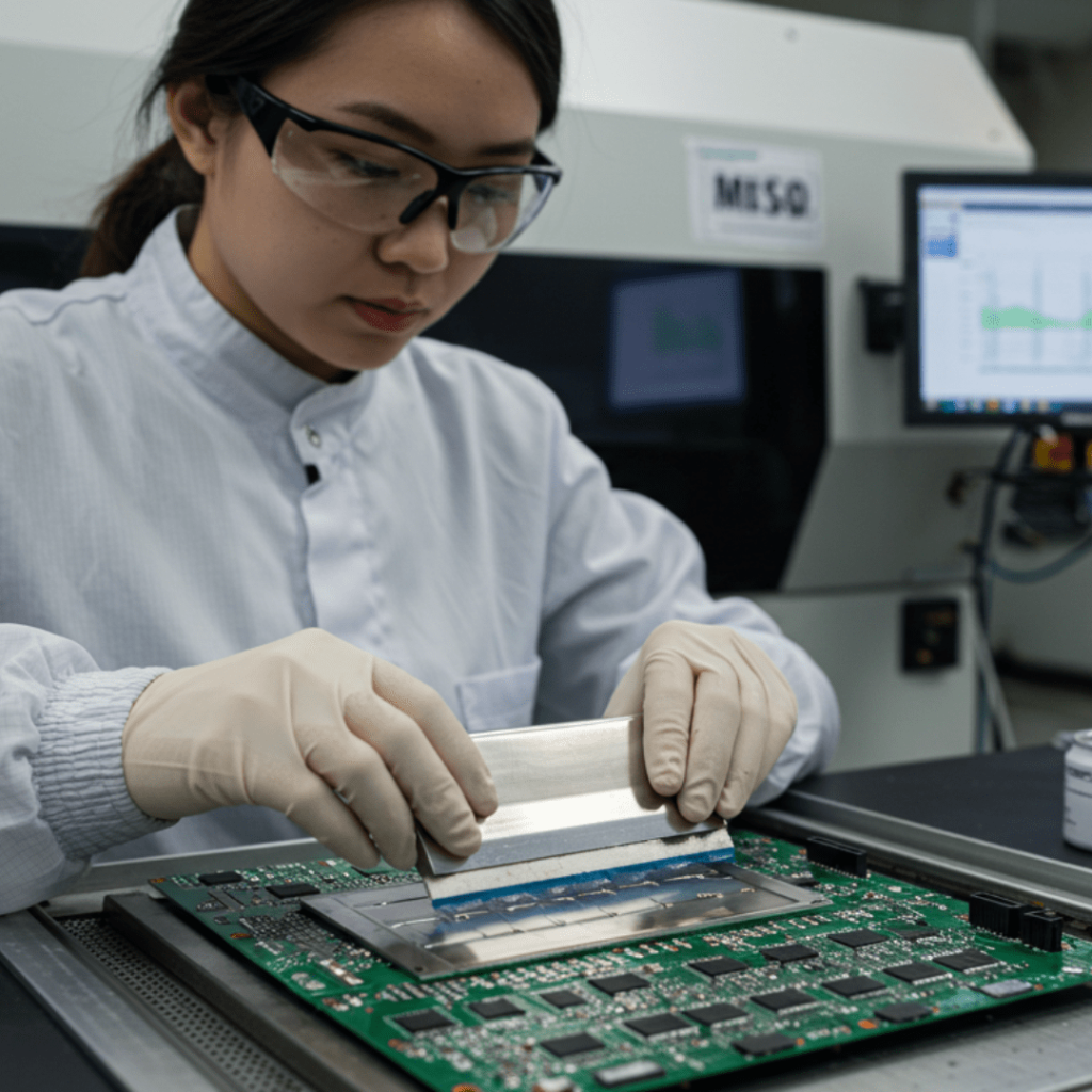
We support conformal coating and selective coating using acrylic, silicone, or urethane materials applied via spray, dip, or selective coating equipment, with masking, cure profiles, and thickness targets defined per drawing or IPC-CC-830 guidelines. Depanelization is handled by routing, V-cut, or laser systems as appropriate to the panel design, minimizing mechanical stress on
Post-assembly, we provide labeling, custom packaging inserts, and simple box-build or sub-assembly integration to deliver plug-in-ready units. ESD-safe handling practices, including grounded workstations, ionization where needed, and antistatic/ESD/MBB packing configurations, are maintained from first operation through final cartoning so sensitive assemblies arrive with both mechanical and electrostatic protection in place.
The benefits of partnering with a Chinese PCB turnkey assembly manufacturer like OurPCB include establishing local supply chains, faster time-to-market, certified quality, and an engineering team that’s highly experienced. Our Chinese turnkey assembly services offer a cost-effective solution for start-ups and enterprises that want quality and the ease of doing business with a PCB assembly company.
Consolidated Chinese Supply Chain
- Single, integrated Chinese supply chain partner for your PCB fabrication, with authorized component sourcing, and turnkey assembly that reduces vendor handoffs and miscommunication.
- Benefit from a centralized demand forecasting and material requirements planning (MRP), which helps minimize excess inventory, component shortages, and resulting production downtime.
- Aggregated order volumes and consolidated shipments from verified distributors lower per-unit component pricing, freight costs, and overall logistics overhead.
Faster Time-to-Market
- Integrated, parallel workflows for PCB fabrication, component procurement, and assembly reduce supplier handoff delays and compress overall project schedules from design to production.
- Fast-track prototype and NPI (new product introduction) lines support urgent development builds, enabling rapid design iteration and earlier validation before volume ramp-up.
- Centralized engineering support and DFM/DFT feedback loops streamline communication, shorten debug cycles, and accelerate issue resolution for faster time-to-market.
Global-ranked Quality
- China offers ISO 9001:2008-certified facilities with IPC-A-600, IPC-A-610, and IPC Class 3 workmanship standards backed by controlled reflow and wave soldering processes, documented temperature profiles, and tightly monitored process parameters.
- Multi-stage inspection and test coverage, including automated optical inspection (AOI), X-ray for BGAs and hidden joints, and optional in-circuit or functional testing, help catch defects early and improve long-term field reliability.
- End-to-end lot-level traceability for boards, components, and test data, with components sourced from authorized distributors, gives you a complete audit trail for quality reporting, failure analysis, and compliance in regulated applications.
Design Flexibility & Engineering Support
- Pre-build DFM/DFT reviews by experienced PCB and test engineers assess manufacturability and test coverage, including stack-up definition, controlled-impedance rules, via strategy, and test-point access, to improve first-pass yield and reduce redesign risk.
- Layout and panel optimization guidance on trace spacing/clearance, drill diameters and annular rings, copper balance, and panelization strategy for multilayer rigid, flex, rigid-flex, high Tg FR4, Rogers, and aluminum PCBs, helping you boost yield and minimize scrap and warpage.
- Lifecycle-aware component engineering support provides recommendations on footprint-compatible or pin-compatible substitutions when parts are obsolete, NRND, or long lead time, along with support for incremental design revisions between prototype spins to keep your BOM robust and buildable.
Mon-Fri: 24 hours,
Sat: 9am-6pm, GMT+8
Reach us at
[email protected]
24 hours online
+86-199-30589219
Mon-Fri: 24 hours,
Sat: 9am-6pm, GMT+8


