Contents
- What is a Circuit Board Made of?
- What are the Components of a PCB?
- Traces
- Pads
- Vias
- Solder Mask
- Silkscreen
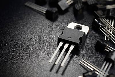
- Electronic Components
- What are the Different Types of Printed Circuit Boards?
- Single-Sided PCBs
- Double-Sided PCBs
- Multi-Layer PCBs
- Flexible, Rigid-Flex, and High-Frequency PCBs
- PCB Classes
- What is the PCB Design Process?
- 1. Schematic Capture
- 2. PCB Layout
- 3. Design Rule Check (DRC)
- 4. Manufacturing Files Preparation
- Which Factors Should Be Considered When Designing PCBs?
- What is the PCB Manufacturing Process?
- 1. Copper Laying And Photoresist Application
- 2. Drilling Of Mounting Holes And Vias
- 3. Application of Solder Mask
- 4. Silk-Screening Of Component Identifiers
- Other PCB Manufacturing Processes
- How does the PCB Assembly (PCBA) Process Work?
- Surface-Mount Technology (SMT)
- Through-Hole Technology (THT)
- Mixed Technology
- The PCB Assembly Process
- FAQs on What is a PCB?
- Are PCBs Eco-Friendly?
- Are There Safety Standards for PCBs?
What is a Circuit Board Made of?
A PCB circuit consists of a base layer (substrate), which can be made from various different materials. The substrate forms the base of the PCB and provides structural support. It’s usually made from insulating materials, like:
- FR-4: A common fiberglass-reinforced epoxy laminate used for general electronics due to its strength and heat resistance.
- CEM-1 and CEM-3: Composite materials that combine fiberglass and paper, typically found in less expensive boards.
- Flexible Substrates: Made from polyimide or polyester for flexible PCBs, used in devices like smartphones and wearables. Polyimide offers excellent heat resistance and flexibility, making it ideal for high-performance applications, while polyester is cost-effective and suitable for mass-produced devices.
- Metal-Core Substrates: Include aluminum or copper for high-performance boards needing better heat dissipation, such as LED lighting. These substrates, commonly used in metal core PCBs, are designed to enhance thermal management in various applications.
What are the Components of a PCB?
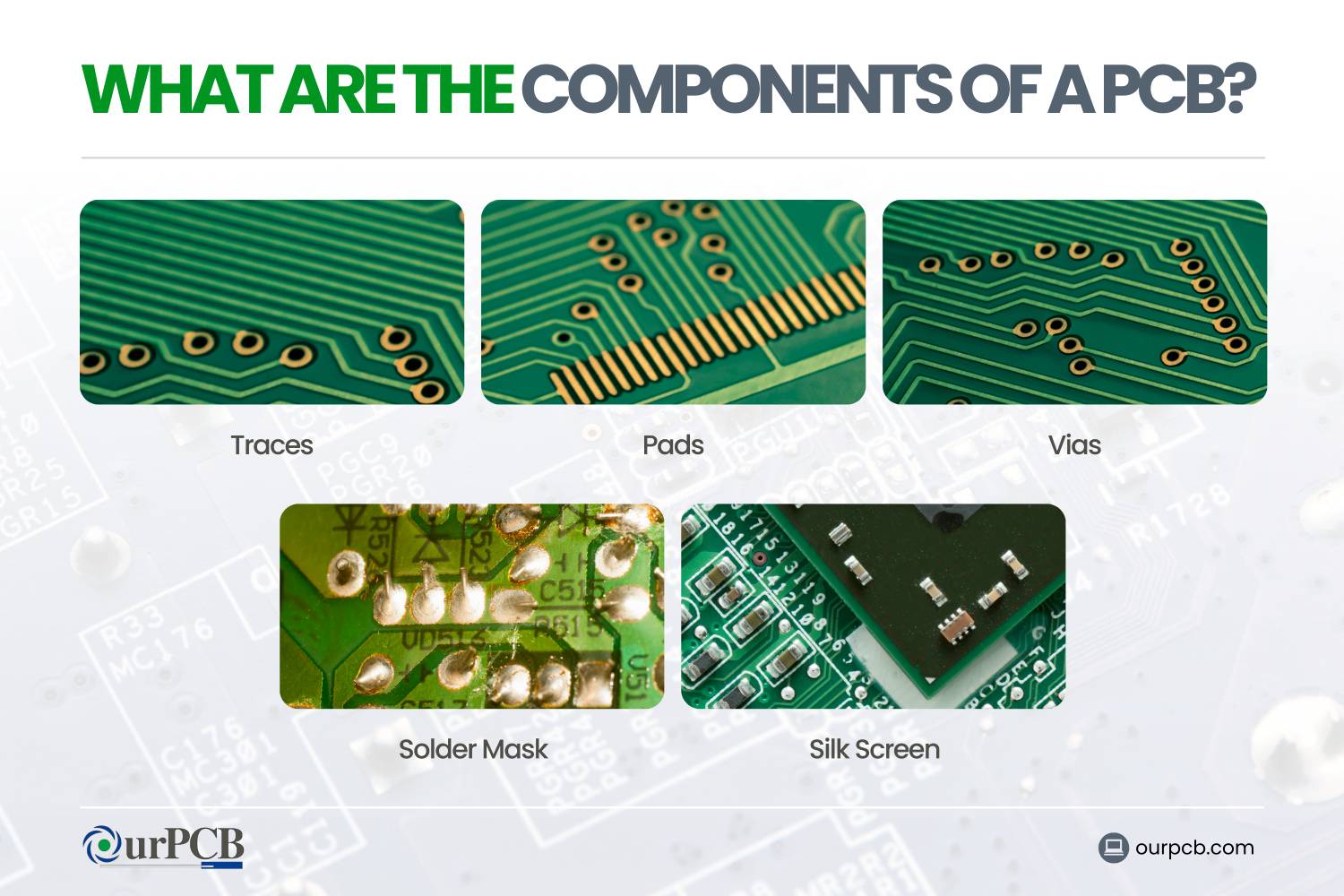
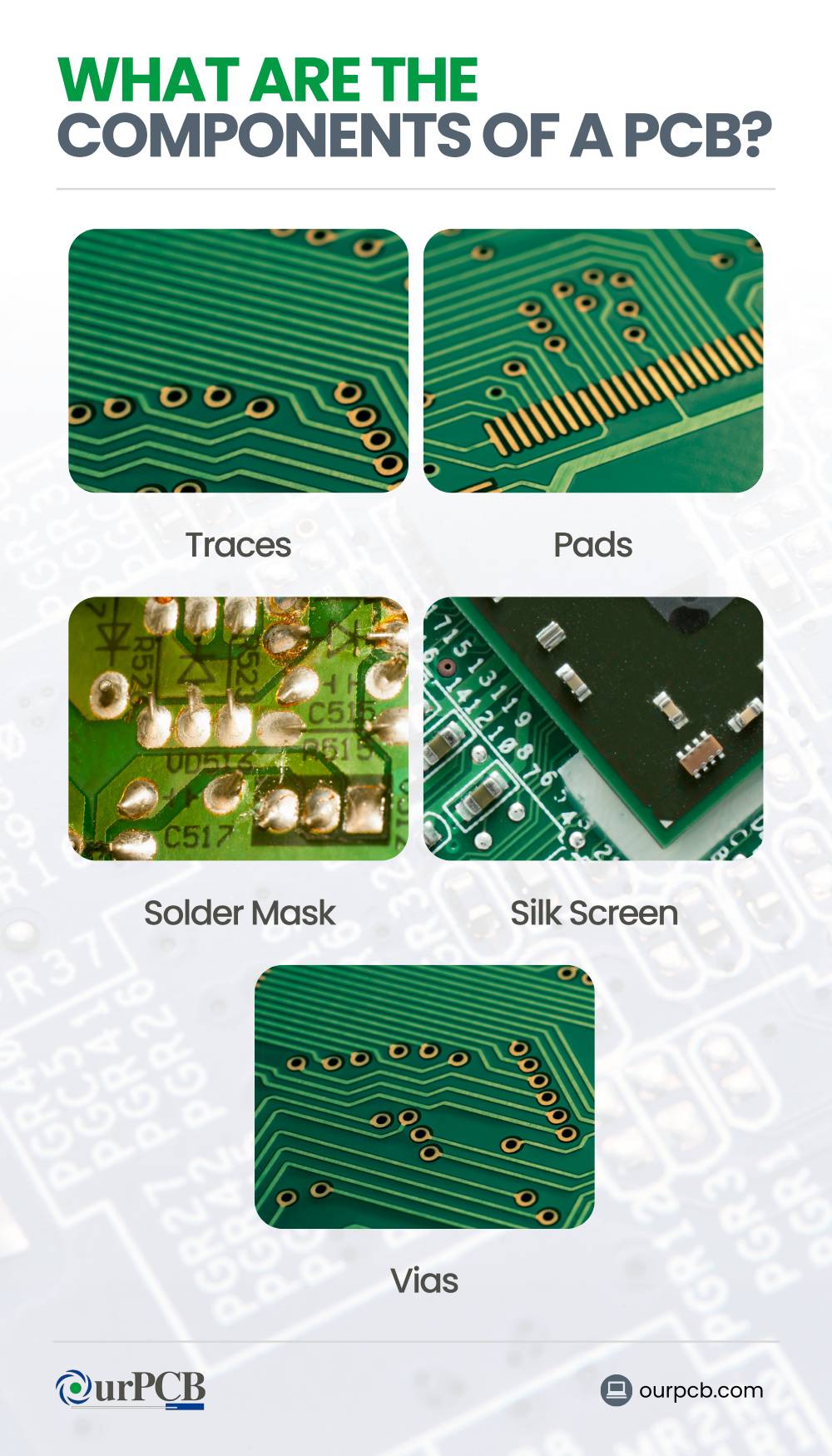
Apart from the substrate, a printed PCB includes a range of other components. These include traces, pads, vias, solder mask, silkscreen, and various electronic components.
Traces
PCB Traces are pathways etched into the copper layers of a PCB for electricity to flow between components. They’re designed to handle specific amounts of current and to reduce electrical interference.
Traces are located on the surface or internal layers of the board, depending on its complexity. In multi-layer boards, traces can run on multiple levels to connect different areas without overlapping.
Pads
PCB Pads are small, metallic areas where electronic components are soldered and mounted onto the board. They act as the connection points between the components and the copper traces on the board, enabling electrical signals to flow throughout the circuit board design.
- Through-Hole Pads: These surround holes in the PCB where components like resistors or capacitors have leads that pass through the board.
- Surface-Mount Pads: These are flat areas of copper on the surface of the board where components are soldered directly, common on compact designs.
Vias
PCB Vias are small, drilled holes in a PCB filled or coated with conductive material, such as copper. They create electrical pathways between different layers of the board, allowing signals and power to travel from layer to layer. This makes it possible to design compact layouts and complex circuits while keeping the board reliable.
There are three main types of vias:
- Through-Hole Vias: These pass through the entire PCB, connecting all layers.
- Blind Vias: These connect the surface layer to one or more internal layers but don’t go all the way through the board.
- Buried Vias: These are entirely within the internal layers, hidden from the outer surface.
Solder Mask
The solder mask is a protective layer that covers the copper traces on a PCB. It prevents short circuits, shields the copper from damage or corrosion, and guides solder to the correct areas during assembly. Solder masks are usually green but can come in other colors as well.
Silkscreen
The silkscreen is a printed layer on top of the solder mask. It uses white or other colored ink to display helpful information like:
- Component labels.
- Part numbers.
- Company logos or assembly guides.
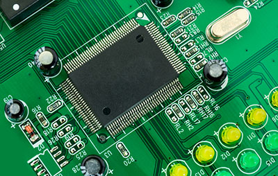
Electronic Components
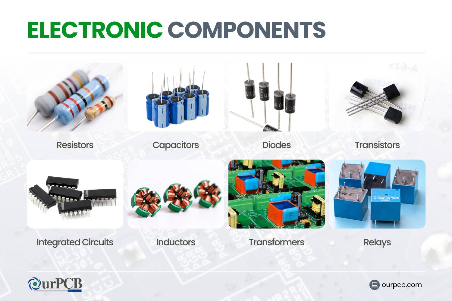
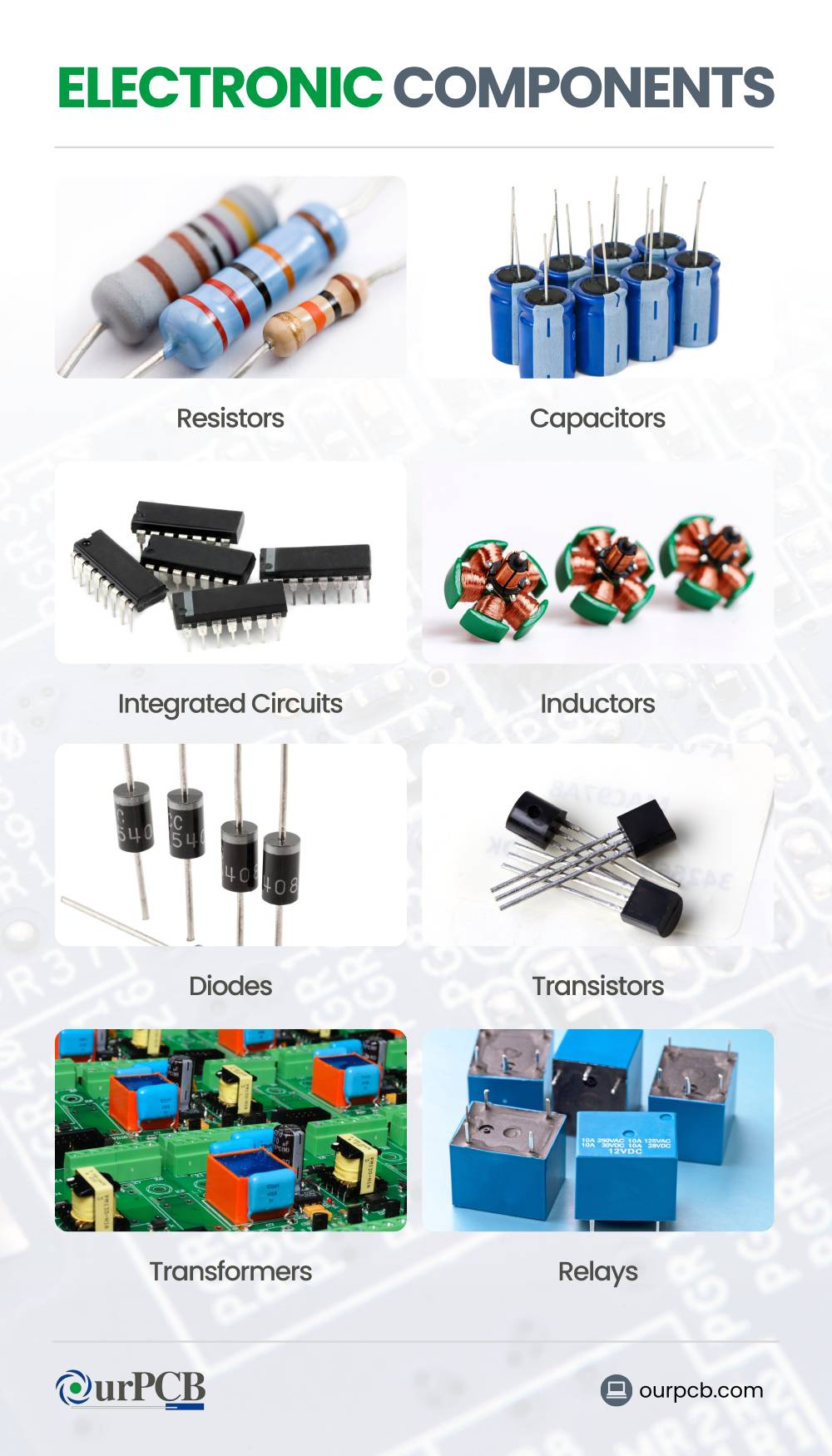
A PCB holds components like resistors, capacitors, diodes, transistors, ICs, inductors, transformers, and relays. These components are mounted on the board and work together to control electricity and make the circuit function.
- Resistors: These limit the flow of electrical current, protecting other parts from damage due to excessive current.
- Capacitors: Capacitors store and release electrical energy, helping to smooth out voltage fluctuations and maintain a steady power supply. They consist of two conductive plates separated by a dielectric material, allowing them to accumulate charge when connected to a power source.
- Diodes: Diodes allow current to flow in one direction only, preventing potential damage from reverse currents.
- Transistors: Transistors act as switches or amplifiers, controlling the flow of electrical signals and enabling complex operations within the circuit.
- Integrated Circuits (ICs): ICs are compact assemblies of electronic components, such as transistors and resistors, that perform specific functions like processing data or managing power.
- Inductors: Inductors store energy in a magnetic field when electrical current passes through them, filtering signals and managing frequencies within the circuit.
- Transformers: Transformers transfer electrical energy between circuits, adjusting voltage levels to meet the needs of different components.
- Relays: Relays are electrically operated switches that control the flow of current in a circuit, allowing a low-power signal to manage a higher-power circuit.
What are the Different Types of Printed Circuit Boards?
| Types of PCBs | Description | Advantages | Disadvantages | Common Uses |
|---|---|---|---|---|
| Single-Sided PCB | One layer of conductive material, used for simple designs. | Low cost, simple manufacturing. | Limited to simple circuits, low durability. | Consumer electronics like calculators and remote controls. |
| Double-Sided PCB | Features conductive layers on both sides, allowing for more complex circuits. | Supports moderate complexity, good for industrial use. | More costly and complex than single-sided. | Industrial controls, power supplies, and automotive dashboards. |
| Multi-Layer PCB | Contains three or more layers for high-density and advanced applications. | Compact design for complex circuits, supports high performance. | Expensive and requires precise manufacturing. | Medical devices, telecommunications, and computers. |
| Flexible PCB | Made from flexible materials, suitable for compact or movable devices. | Can fit into tight spaces and withstand bending. | Less durable than rigid PCBs, limited support for heavy components. | Wearables, cameras, and mobile phones. |
| Rigid-Flex PCB | Combines rigid and flexible layers, offering both durability and adaptability. | Combines the benefits of rigid and flexible PCBs, reduces connectors. | Costly to produce, requires advanced design skills. | Aerospace, military systems, and advanced medical devices. |
| High-Frequency PCB | Designed for high-speed signals, ideal for telecommunications and RF devices. | Handles high-frequency signals with minimal interference. | High manufacturing cost, sensitive to precise material specifications. | Satellite systems, radar, and wireless communication devices. |
Single-Sided PCBs
Single-sided PCBs have one layer of conductive material, usually copper, on one side of the board. They’re simple to manufacture and cost-effective, making them a good choice for straightforward designs. These boards are used in products like calculators, LED lighting, and low-power circuits.
Double-Sided PCBs
Double-sided PCBs have conductive layers on both sides of the board, so components can be mounted on either side. These two layers are connected, enabling signals and power to move between them. This design supports more advanced circuit layouts and is commonly used in amplifiers, automotive systems, and industrial controls.
Multi-Layer PCBs
Multi-layer PCBs have three or more conductive layers separated by insulating materials. These layers are stacked together, creating a compact design that supports complex circuits. Connections between the layers allow signals and power to flow efficiently across the board.
Flexible, Rigid-Flex, and High-Frequency PCBs
Flexible PCBs
Made from bendable materials like polyimide, these boards can fold or twist, making them ideal for compact devices like smartphones, wearables, and medical tools. Their flexibility also allows them to handle movement and vibration.
Rigid-Flex PCBs
These combine rigid and flexible layers in a single board, offering both stability and adaptability. They’re used in aerospace, military equipment, and consumer electronics where space and reliability are both important. This design reduces the need for connectors and simplifies assembly.
High-Frequency PCBs
Built to handle high-speed signals, these boards are used in satellites, radar systems, and microwave communication. Specialized materials keep the signal integrity strong and have excellent performance at high frequencies.
Special Offer: Get $100 off your order!
Email [email protected] to get started!
PCB Classes
Printed circuit boards are categorized into classes based on their quality and reliability standards, as defined by the IPC (Association Connecting Electronics Industries). These classifications help manufacturers and designers make sure that PCBs meet the specific requirements of their intended applications.
| Class | Purpose | Example |
|---|---|---|
| Class 1: General Products | For products focused on basic function, where long life or continuous use is not needed. | Toys, remote controls, household appliances. |
| Class 2: Service Products | Designed for devices that need steady performance and a longer lifespan, but not constant operation. | Laptops, smartphones, routers, industrial systems. |
| Class 3: High-Reliability Products | Built for critical applications that demand nonstop reliability and no downtime. | Medical devices, satellites, military and aerospace components. |
What is the PCB Design Process?
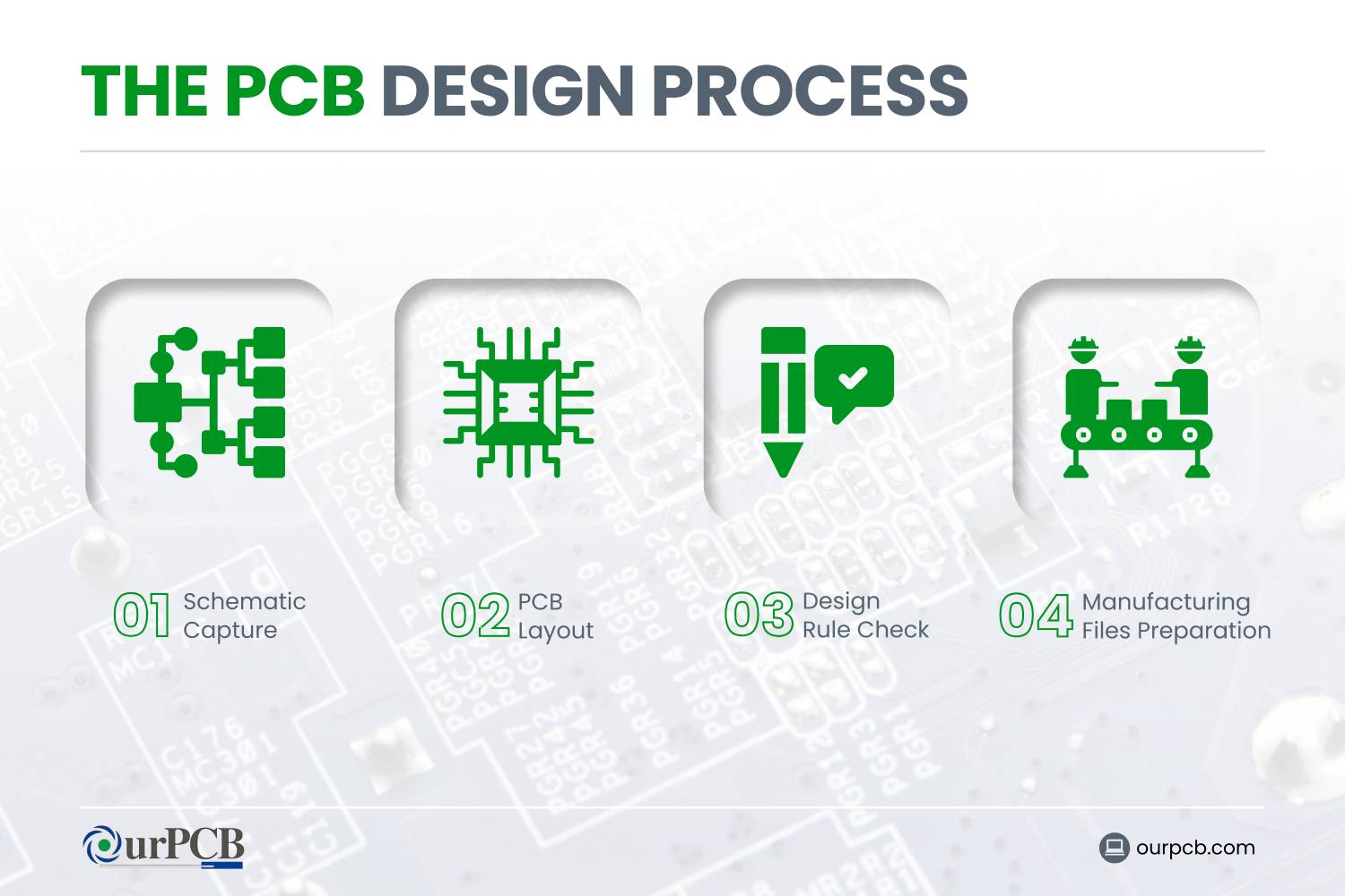
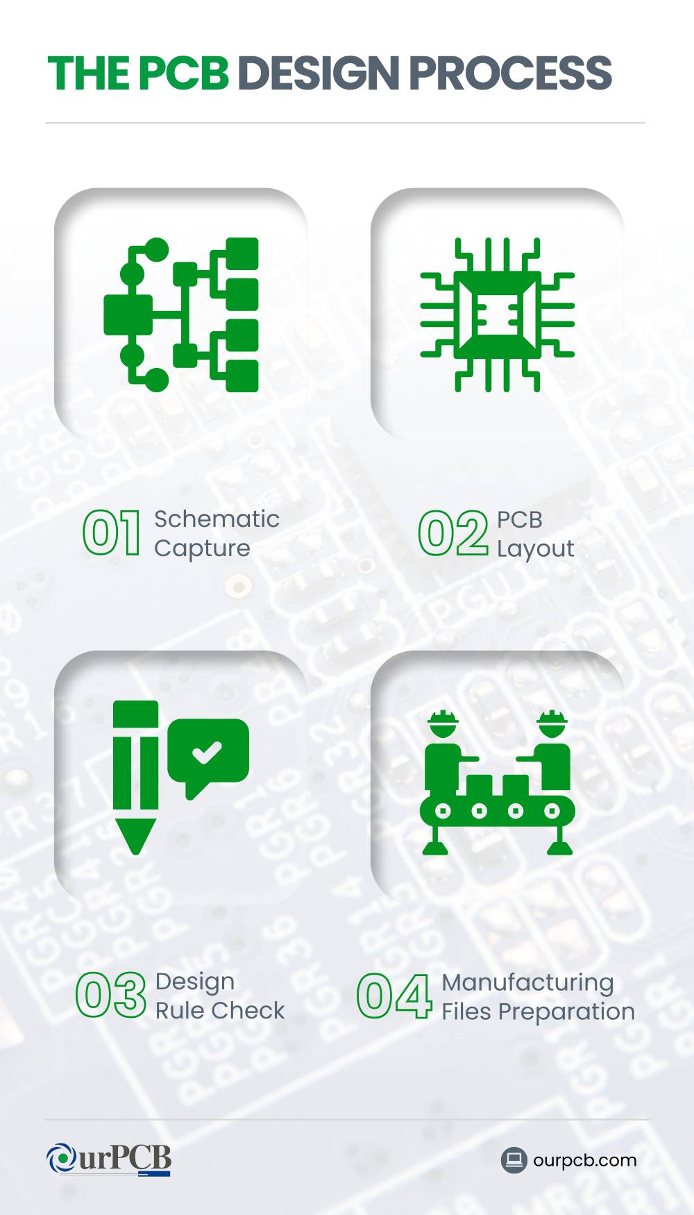
The PCB design process includes creating a schematic, arranging components and routing connections, checking for design compliance, and preparing manufacturing files.
1. Schematic Capture
The process begins with creating a detailed schematic diagram using specialized design tools and software. This diagram represents the electrical connections between components, serving as a blueprint for the PCB layout.
2. PCB Layout
After the schematic is complete, the components are arranged on the board, and traces are routed to connect them. For the layout to be effective, a well-designed PCB layout ensures optimal signal flow, heat dissipation, and ease of manufacturing.
3. Design Rule Check (DRC)
Once the layout is complete, a Design Rule Check is performed to verify that the PCB design meets the specified manufacturing constraints and industry standards. The DRC identifies issues like spacing violations, trace width errors, and other potential problems that could affect the board's functionality or manufacturability.
4. Manufacturing Files Preparation
In this final step, Gerber files, drill files, and the Bill of Materials (BOM) are created. These files contain all the details manufacturers need to produce the PCB accurately and efficiently.
Which Factors Should Be Considered When Designing PCBs?
Designing PCBs involves managing heat, reducing interference, maintaining signal quality, and meeting mechanical requirements to achieve reliable performance.
Thermal Management
Managing heat is important to prevent overheating and protect components. Heat-generating parts should be placed away from sensitive components to avoid thermal interference. Thermal vias can help transfer heat to internal layers or heat sinks, while large copper planes are often used to dissipate heat effectively. For high-power applications like LED lighting systems, specialized LED PCB thermal management techniques become essential to maintain optimal performance and component longevity.
Electromagnetic Interference (EMI)
Reducing EMI helps avoid signal disruptions and interference. Continuous ground planes minimize noise, while keeping high-speed signal traces short and direct lowers radiation. Shielding techniques can also protect sensitive parts from external interference.
Signal Integrity
Signal integrity makes sure circuits function as expected. This involves controlling factors like impedance matching, minimizing propagation delays, and reducing crosstalk between signal traces. For tips on maintaining robust signal performance, check out this guide on how to avoid signal integrity problems.
Mechanical Constraints
Physical design and durability are shaped by mechanical factors. Boards must fit within their enclosures, with mounting holes placed to prevent stress. Connectors should be positioned for easy access while avoiding strain on solder joints.
What is the PCB Manufacturing Process?
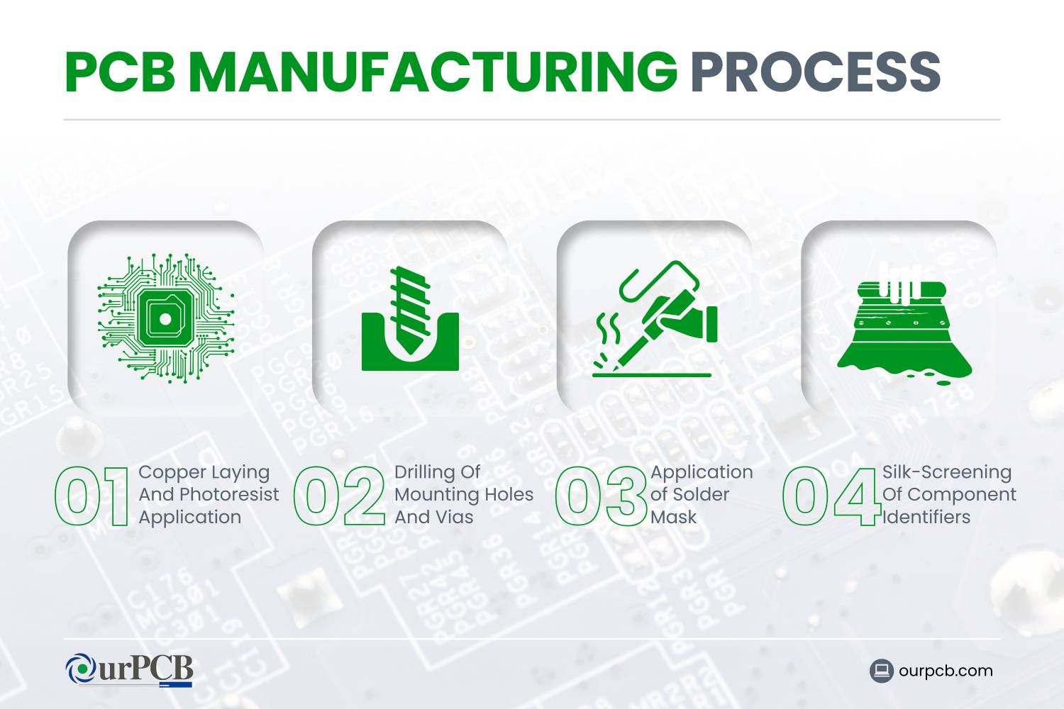
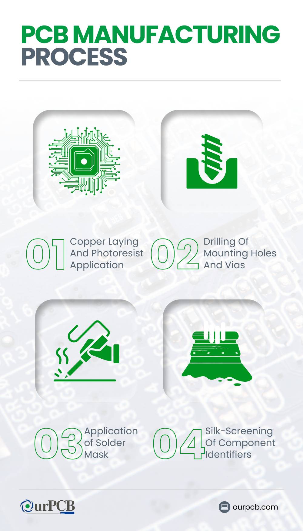
The PCB manufacturing process involves creating circuit patterns, drilling holes, applying protective layers, and finishing the board to prepare it for assembly and use.
1. Copper Laying And Photoresist Application
The process begins with laminating a thin copper layer onto the substrate material. A photoresist, which is a light-sensitive material, is then applied over the copper surface. This layer will be used to define the circuit pattern during the exposure process.
2. Drilling Of Mounting Holes And Vias
Precision drilling is performed to create holes for component leads and vias, which are pathways that allow electrical connections between different layers of the PCB. These holes are drilled using computer-controlled machines for accuracy.
3. Application of Solder Mask
A solder mask is applied over the entire board, except for the areas that will be soldered. This protective layer prevents solder bridges between conductive traces and protects the copper from oxidation. The solder mask also gives the PCB its characteristic color, usually green.
4. Silk-Screening Of Component Identifiers
The silkscreen layer is added to print component identifiers, symbols, and other markings on the PCB surface. This step aids in the printed circuit board assembly process and helps technicians identify components during maintenance or repair.
Other PCB Manufacturing Processes
PCBs may undergo these processes too, depending on the type of PCB they are and their purpose.
Etching
Etching removes unwanted copper from the board to create the desired circuit pattern. This is usually done using chemical solutions that dissolve the excess copper, leaving only the necessary traces.
Lamination
For multi-layer PCBs, lamination is used to bond multiple layers of substrate and copper together under heat and pressure. This process creates a single, solid board with multiple conductive layers, allowing for more complex circuit designs.
Surface Finishing
Surface finishing involves applying a protective coating to the exposed copper areas to prevent oxidation and improve solderability. Common surface finishes include:
- Hot Air Solder Leveling (HASL): The board is dipped in molten solder, and excess is removed with hot air to create a uniform coating.
- Electroless Nickel Immersion Gold (ENIG): A thin layer of nickel is coated with a layer of gold, providing a flat surface and good oxidation resistance.
- Organic Solderability Preservative (OSP): An organic compound is applied to protect the copper surface until soldering.
How does the PCB Assembly (PCBA) Process Work?
The custom PCB assembly (PCBA) process involves placing electronic components onto the surface of a PCB, soldering them in place, and inspecting the board to make sure it functions correctly.
Surface-Mount Technology (SMT)
Surface mount technology involves mounting components directly onto the surface of the PCB. This method allows for smaller components and higher circuit densities, making it suitable for compact devices like smartphones and laptops.
Through-Hole Technology (THT)
THT requires inserting PCB component leads through pre-drilled holes in the PCB and soldering them on the opposite side. This technique provides strong mechanical bonds, making it ideal for components that may experience physical stress, like connectors and large capacitors.
Mixed Technology
Mixed technology combines both SMT and THT on a single PCB. This approach leverages the advantages of both methods, allowing for complex designs that require both high-density components and robust mechanical connections.
The PCB Assembly Process
1. Component Placement
The assembly process begins with placing components onto the PCB. In SMT, automated machines precisely position surface-mount devices onto solder paste-applied pads. For THT, components are manually or robotically inserted into the drilled holes.
2. Soldering
Once components are placed, soldering secures them to the PCB. Common soldering techniques include:
- Reflow Soldering: Used mainly for SMT, the PCB with components passes through a reflow oven where the solder paste melts and solidifies, forming electrical connections.
- Wave Soldering: Mostly used for THT, the PCB is passed over a wave of molten solder, which attaches the component leads to the board.
- Selective Soldering: Used when only specific areas of the PCB require soldering, such as in mixed technology assemblies.
3. Inspection & Testing
After soldering, the assembled PCB undergoes inspection and testing to verify functionality and quality. Methods include:
- Automated Optical Inspection (AOI): Cameras scan the board to detect issues like missing components or solder defects.
- X-ray Inspection: Used to examine hidden solder joints, especially in complex assemblies.
- Functional Testing: The PCB is tested under operating conditions to make sure it performs as intended.
FAQs on What is a PCB?
Are PCBs Eco-Friendly?
PCBs are not naturally eco-friendly because of the materials and chemicals used in their production. Regulations like RoHS (Restriction of Hazardous Substances) and WEEE (Waste Electrical and Electronic Equipment) help reduce their environmental impact by limiting harmful materials and promoting recycling.
Are There Safety Standards for PCBs?
Yes, there are established safety standards for Printed Circuit Boards (PCBs) to maintain quality and reliability. Organizations like IPC (Association Connecting Electronics Industries) and ISO (International Organization for Standardization) have developed guidelines that manufacturers follow. Sticking to these standards helps prevent defects, reduces the need for rework, and enhances customer satisfaction.
At OurPCB, we meet RoHS standards for lead-free soldering, as well as meeting all printed circuit board industry standards.
Back to Top: What is a PCB?
Special Offer: Get $100 off your order!
Email [email protected] to get started!