Layers: 2L+Copper substrate
Thickness: 3.2mm
Surface finish: Immersion gold
Outler layer copper thickness: 6oz
Layers: 2L
Thickness: 6.0mm
Min. hole size: 0.6mm
Outler layer copper thickness: 2oz
2 Layers PCB Structure
Our 2 layers PCB design features a complete stack-up that includes:
- Top Copper Layer – Primary signal routing and component placement
- Dielectric Core – FR-4 substrate providing insulation and mechanical support
- Bottom Copper Layer – Additional routing and ground plane
- Solder Mask – Protective coating on both sides
- Silkscreen – Component identification and markings
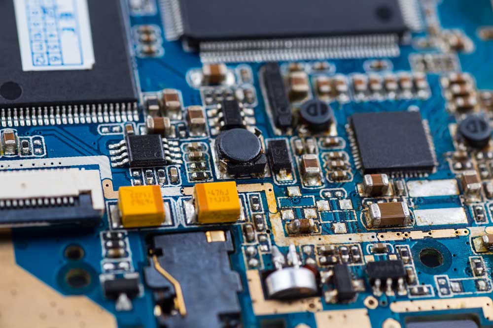
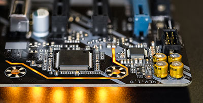
Integrated Circuit Board of a Hard Disk
2 Layers PCB Stack-Up and Design
As an experienced 2 layers PCB manufacturer, OurPCB provides optimized stack-up configurations for maximum performance:
Standard 2 Layers PCB Stack-Up
- Layer 1 (Top): Signal layer with component mounting
- FR-4 Core: Dielectric material with controlled thickness
- Layer 2 (Bottom): Ground/power plane or additional signal routing
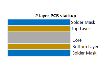
2 layer PCB stack-up
Critical Design Elements for 2 Layers PCB
- Signal Integrity: Our 2 layers PCB design minimizes crosstalk through proper trace spacing
- Ground Plane: We implement solid ground planes to reduce noise and improve signal return paths
- Power Distribution: Strategic power routing ensures stable voltage delivery
- Component Placement: Optimized for thermal performance and assembly efficiency
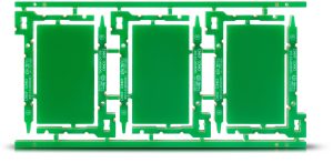
pcb prototyping
2 Layers PCB Thickness
As a professional 2 layers PCB manufacturer, OurPCB offers various thickness options to meet your specific requirements:
- Standard Thickness: 1.6mm (0.063″)
- Thin Profile Options: 0.8mm, 1.0mm, 1.2mm
- Thicker Options: 2.0mm, 2.4mm
The thickness of your 2 layers PCB impacts several performance factors:
- Mechanical Stability: Thicker boards provide better mechanical support
- Electrical Performance: Controlled impedance for high-frequency applications
- Thermal Management: Heat dissipation characteristics
- Weight Considerations: Critical for mobile and aerospace applications

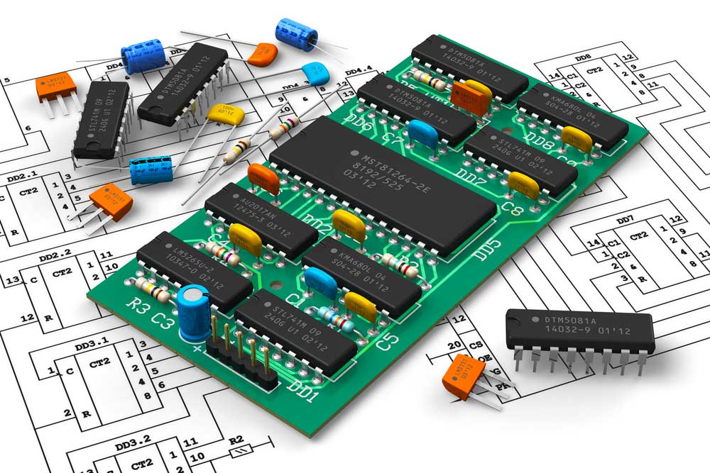
Electronic printed circuit boards
2 Layers PCB Manufacturing Process
At OurPCB, our 2 layers PCB manufacturing process follows these precise steps:
- Material Preparation: Selection of premium copper-clad laminates
- Imaging: Precision photolithography to define circuit patterns
- Etching: Controlled copper removal to create circuit traces
- Drilling: CNC precision drilling for component holes and vias
- Metallization: Copper plating of holes for layer interconnection
- Solder Mask Application: Protection of conductive traces
- Surface Finish: Application of chosen final finish (HASL, ENIG, etc.)
- Silkscreen Printing: Component identification markings
- Electrical Testing: 100% E-test to verify circuit integrity
- Final Inspection: Dimensional and visual quality checks
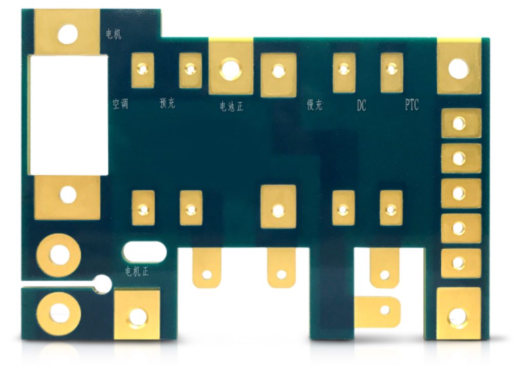
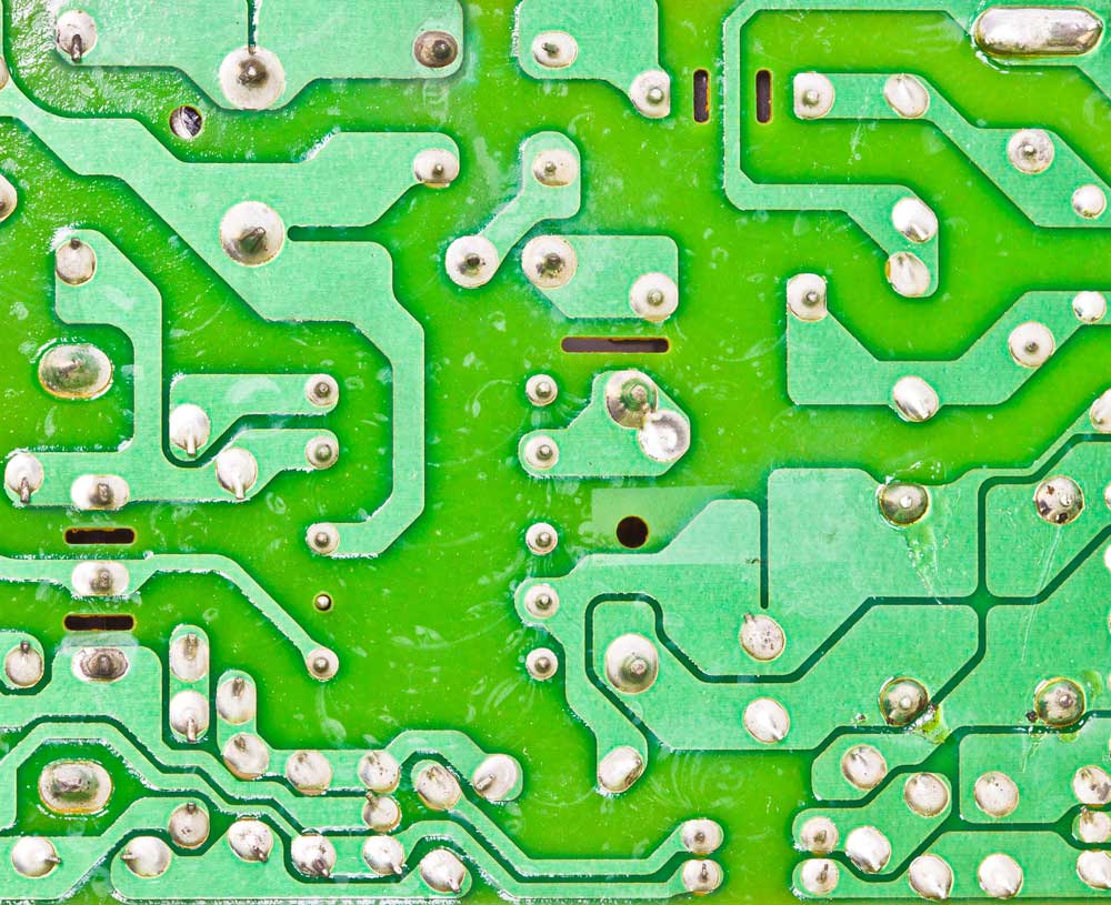
Electronic printed circuit board bottom layer
2 Layers PCB Cost Factors
As a competitive 2 layers PCB manufacturer, OurPCB optimizes costs while maintaining quality:
- Board Size: Price typically ranges from $1-$5 per square inch for standard orders
- Quantity: Significant discounts available for higher volume orders
- Design Complexity: Features like controlled impedance affect pricing
- Material Selection: Standard FR-4 vs. specialized materials
- Surface Finish: HASL is most economical; ENIG offers superior performance
- Turnaround Time: Expedited services available at premium rates
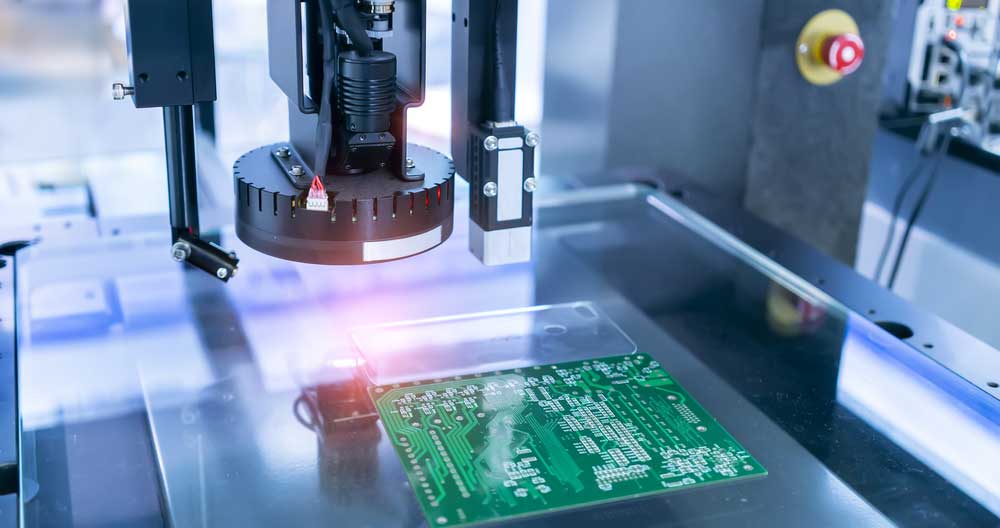
Vision measuring instrument inspecting PCB circuit board
Special Offer: Get $100 off your order!
Email [email protected] to get started!
2 Layers PCB vs. 4 Layers PCB: Making the Right Choice
As both a 2 layers PCB manufacturer and multi-layer specialist, OurPCB provides guidance on selecting the optimal board type:
2 Layers PCB Advantages:
- Cost-Effective: 30-50% lower production costs
- Simpler Manufacturing: Faster turnaround times
- Sufficient for Many Applications: Ideal for less complex circuits
- Easier Prototyping: Quicker design iterations
- Thinner Profile Options: When space constraints are critical
When to Consider 4 Layers PCB:
- Complex routing requirements
- High-speed digital circuits
- Improved EMI/RFI performance needs
- Dense component placement
- Dedicated power and ground planes required
Digital circuit board with microchips
Applications of 2 Layers PCB
Our 2 layers PCB manufacturing services support diverse applications:
Consumer Electronics
- Computer peripherals
- Tablets and smartphones
- Home appliances
- Audio equipment

Industrial Applications
- Control systems
- Power supplies
- Instrumentation
- Monitoring equipment
Automotive Electronics
- Dashboard controls
- Lighting systems
- Sensor interfaces
- Entertainment systems
Medical Devices
- Patient monitoring
- Diagnostic equipment
- Non-critical medical devices
- Laboratory instruments
Electronic circuit board

Using the computer
Single-Sided vs. 2 Layers PCB
Understanding the differences helps select the right board for your application:
Single-Sided PCB
- Components and traces on one side only
- Limited routing capabilities
- Lower manufacturing cost
- Simpler design requirements
- Suitable for very basic circuits
2 Layers PCB (Double-Sided PCB)
- Components and traces on both sides
- Significantly more routing space
- Greater design flexibility
- Better signal integrity
- Higher component density
- More challenging thermal management
Benefits of 2 Layers PCB
As a premier 2 layers PCB manufacturer, OurPCB’s double-sided boards offer significant advantages:
- Increased Routing Capacity: Components and traces on both sides maximize available space
- Design Flexibility: More options for component placement and trace routing
- Compact Size: Smaller footprint compared to single-sided designs
- Improved Signal Integrity: Better control of impedance and crosstalk
- Cost-Effective Complexity: More capable than single-sided without the cost of multi-layer boards
- Reliability: Proper ground planes improve electrical performance and stability
- Versatility: Suitable for a wide range of applications from simple to moderately complex
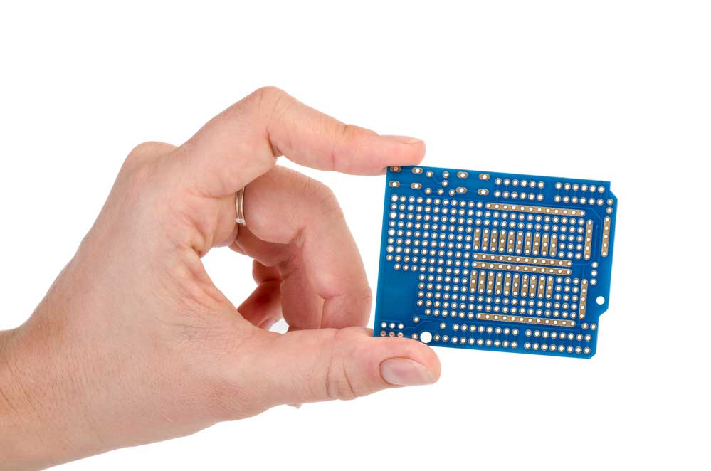
Blue prototyping PCB in a hand
How to Choose Between 2 Layers PCB and Multi-Layer Options
When working with OurPCB as your 2 layers PCB manufacturer, consider these factors:
Project Factors to Consider:
- Budget Constraints: 2 layers PCBs are more economical
- Circuit Complexity: Component count and routing density
- Signal Integrity Requirements: High-speed signals may need additional layers
- Size Limitations: Smaller boards may require additional layers for routing
- Thermal Considerations: Heat dissipation needs
- Electromagnetic Interference: Shielding requirements
- Production Timeline: 2 layers PCBs typically have faster turnaround
- Expected Product Lifespan: Reliability requirements
Why Choose OurPCB as Your 2 Layers PCB Manufacturer
OurPCB delivers exceptional value through:
- Engineering Expertise: Design review and optimization support
- Quality Materials: Premium substrates and copper foils
- Advanced Equipment: State-of-the-art manufacturing technology
- Rigorous Testing: 100% electrical testing and visual inspection
- Flexible Options: Customized solutions for your specific requirements
- Competitive Pricing: Excellent value without compromising quality
- Fast Turnaround: Expedited services when you need them most
- Dedicated Support: Professional assistance throughout your project
Request Your 2 Layers PCB Quote Today
Partner with OurPCB, your trusted 2 layers PCB manufacturer, for exceptional quality, competitive pricing, and superior service.
Special Offer: Get $100 off your order! No hidden fees and no minimum order quantity required.
Complete our simple quote form:
- Select your PCB type (Rigid PCB for 2 layers PCB)
- Indicate your production volume
- Upload your Gerber files
- Provide your contact information
Our expert team will respond promptly with a competitive quote tailored to your specific 2 layers PCB requirements.
Back to Top: 2 Layers PCB
Special Offer: Get $100 off your order!
Email [email protected] to get started!