Printed circuit boards (PCBs) have existed for almost a century. This demonstrates their relevance in electronic circuit systems.
For this reason, the demand for small and high-density PCBs is increasing yearly in the digital era.
Nowadays, creating the smallest circuit board sizes is facilitated by the use of cutting-edge manufacturing technologies.
While PCB manufacturing consists of different dimensions, tools, and materials, it heavily relies on Gerber files.
So, what are Gerber files? How do you generate Gerber files? This article contains the answers to these questions and other features of Gerber files.
Welcome to the step-by-step guide on how to generate Gerber files.
Contents
- What Is a Gerber File for PCB
- What Should the PCB Gerber File Contain?
- Pads and copper traces on the upper and lower layers:
- Continuous Copper Connections:
- Drill Hole Patterns and Location:
- Drill Hit Markings:
- Buried and Hidden Vias:
- Solder mask layers:
- Silkscreen Layers:
- Circuit Board Surface Treatment:
- Board Outline and Dimensions:
- PCB Panelization:
- Gerber File Formats
- RS274-D
- RS274X
- ODB++
- Gerber X2
- Gerber X3
- Essential Features of a Gerber File Viewer
- How to Make PCB Gerber Files
- Kicad- Kicad Exporter Gerber
- Open your .kicad_pcb file.
- Plot your Kicad PCB as Gerber Files
- Generate the Drill
- Check the Gerber Files in Gerber View
- Compress your Files in a Single .zip File.
- Altium Designer- Altium Gerber Files
- After creating a new Gerber Output alternative
- Eagle- Eagle Gerber Files
- Generate Drill Files
- Generate Gerber Files
- Compress your files in a .zip File.
- The Importance of Gerber Files in PCB Manufacturing
- PCB Gerber Standard File Extension
- How to Open GBX Files
- Conclusion
What Is a Gerber File for PCB
As mentioned earlier, a Gerber file is one of the essential elements of PCB design.
The name originates from Gerber Systems Corp- the first company to develop Gerber files.
It refers to the PCB features, like solder mask layers, legend, drill template, etc.
Typically, you will design your PCB in CAD systems that use manufacturing information to produce two or three-dimensional circuit board designs.
Likewise, you need to enter data into these systems to create the designs.
Does this sound simple? You may think it is a system automatically making designs upon entering the data.
However, that is not true, as you have to refer to Gerber file guidelines while keying in the information.
Gerber files define the requirements in every product development step.
Remember, you can use these files for circuit board fabrication and assembly.
What Should the PCB Gerber File Contain?
PCB Gerber files should have the following data for precise circuit board manufacturing.
Pads and copper traces on the upper and lower layers:
Most PCBs have copper traces and component pads on the top layer, while ground planes and other internal traces go to the bottom. Gerber files should list this layer data to make it clear to the manufacturer.
Continuous Copper Connections:
Copper pours are broad areas containing continuous copper connections. These pours often make ground planes, and the connections enhance the board’s electrical properties. Gerber file should indicate the pour’s size and location on the top and bottom layers. 
A Gerber file of a PCB layout’s inner layers
Drill Hole Patterns and Location:
The drill files indicate the hole patterns, locations, and sizes, providing critical data about hole drilling in circuit boards.
Drill Hit Markings:
These markings indicate where the drill bit should contact the board, complementing the drill file to ensure precise hole positioning.
These via-holes link different internal layers without going through all of them, meaning they require special manufacturing techniques. Gerber files should include their size and placement data.
Solder mask layers:
Solder mask layering is essential for mass-produced circuit boards that undergo automated soldering (wave and reflow) because it prevents shorting between components, traces, and pads. Gerber files should contain the solder mask coverage data for the upper and lower layers.
Silkscreen Layers:
These layers visually indicate markings for component placement during assembly. On the Gerber file, the data should indicate the size and location of these labels, markings, and symbols.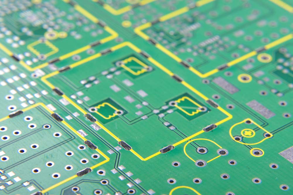
A circuit board with a silkscreen layer
Circuit Board Surface Treatment:
You can include data about the required surface finish on the entire board or specific sections.
Board Outline and Dimensions:
Gerber files must contain the board’s dimensions, shape, connector cutouts, displays, and other outline information.
PCB Panelization:
Panelization involves manufacturing multiple copies of the same PCB design. You can combine Gerber files into a panel for mass manufacturing, and the resulting file should indicate the panel layout and number of copies (PCBs) in each panel.
Panelized PCBs ready for assembly
Gerber File Formats
RS274-D
Developed in the 1960s, RS274-D is the first and oldest Gerber file format. This binary format represents PCB designs as command sets, each with specific instructions and data.The binary information has a rectangular matrix form with dots inside to define the PCB geometry. Each dot contains location and state (on/off) data.
RS274X
Also known as X-Gerber or extended Gerber, RS274X is a revised and enhanced version of the RS274-D format. It introduced aperture definition support, allowing you to save and transfer more complex geometries.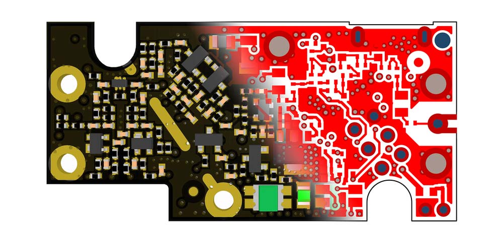
A PCB design concept blending a 3D view with the inner layer Gerber file
Additionally, it enables you to utilize polarity controls, special polygon film commands, film control, and multi-layer structures for single layers.
ODB++
This format is compatible with almost all CAD programs, making it an all-inclusive, self-extracting standardized input format. ODB++ also eliminated human errors by automating stackup, labeling, and drill placement
Gerber X2
Gerber X2 is an improvement of RS274X that allows you to assign attributes to features in the file. The format is compatible with most CAM applications, meaning manufacturers can interpret and implement the saved attributes.For instance, the board’s design can have multiple pads, and Gerber X2 allows you to assign attributes like the pad’s function to these features. You can label them SMD, fiducial, via-pad, etc.
Gerber X3
Introduced in 2020, Gerber X3 uses the same syntax as X2 but includes component information for the top and bottom layers.
Special Offer: Get $100 off your order!
Email sales@ourpcb.net to get started!
Essential Features of a Gerber File Viewer
The Gerber file viewer used by PCB manufacturers should have these features.
- Friendly UI
- Accurate display with pan, rotate, and zoom functions
- Precision tools for measuring design attributes like angles and distance
- Layer control to adjust transparency levels between layers and toggle them on or off
- Compatibility with multiple Gerber file formats
- Multi-file export options (PNG, PDF, etc.)
- Support the latest file format (X3)
- Annotation features
- Compatibility with multiple printers
How to Make PCB Gerber Files
First, you can barely ensure that your manufacturer uses the same software you used in the design process.
If your manufacturer specifies that they are using different software, you should make Gerber files yourself.
Further negotiations and requests will consume your time and affect the manufacturing process significantly.
Still, even if both of you use the same design software, generating Gerber files by yourself is crucial in preventing possible errors resulting from different terms.
Hence, to ensure the production process proceeds as planned and your end products are reliable, you should learn to make Gerber files independently.
Generally, Gerber files come with design information for the conductor, solder mask, and silkscreen layers.
Additionally, regarding the two layers containing similar design information, you should still generate your Gerber files individually to avoid any mix-up.
It is essential to realize that various PCB design tools have distinct operation steps for Gerber file creation.
We will discuss generating Gerber files using Kicad, Altium Designer, and Eagle software.
Kicad- Kicad Exporter Gerber
Generally, it is much easier to create Gerber files via Kicad than other circuit board design tools.
What you need to do is to choose the appropriate layers and make the DRILL file.
Without further ado, let us dive into generating Gebers in Kicad!
Open your .kicad_pcb file.
First, open your Kicad project. Then, double-click the .kicad_pcb template. Press the "PCBNew" tab to open the circuit board editor.
Plot your Kicad PCB as Gerber Files
On your File menu, proceed to the Plot function and select the appropriate layers, as illustrated in the diagram below. Likewise, press the Plot tab to produce the corresponding layers.
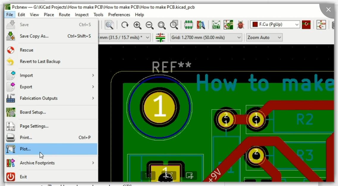
The essential layers you need for a 2-layer circuit board are:
- The upper layer- pcbname.GTL
- The bottom layer- pcbname.GBL
- The solder mask upper layer- pcbname.GTS
- The solder masks the lower layer- pcbname.GBS
- The upper silk layer- pcbname.GTO
- The silk lower layer- pcbname.GBO
- The drill drawing layer- pcbname.TXT
- The board outline layer- pcbname.GML/GKO
Generate the Drill
Another critical point is to create the drill for manufacturing purposes before closing your plot panel.
With this in mind, tick the Suppress leading zones and Minimal header boxes. Then press the Drill File tab, as illustrated below.

That is it. You are done with generating Gerber files!
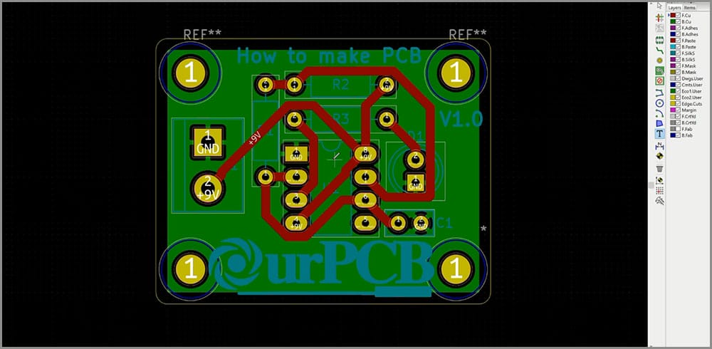
Check the Gerber Files in Gerber View
Though you have finished generating Gerber files, you should confirm whether they function correctly before folding your tools.
Luckily, the process of checking Gerber files is as simple as ABCD. Click the GerbView and confirm the shape and configuration of your PCB. You can send your Gerber file to your PCB manufacturer if everything is OK.
Your board should resemble the image below.
Compress your Files in a Single .zip File.
Lastly, you should compress your files into one .zip file. Besides, you should fill out the document about your board features, such as size.
You can check this video for a comprehensive illustration of exporting Gerber files in Kicad: https://www.youtube.com/watch?v=ncCz7N5ko34.
Altium Designer- Altium Gerber Files
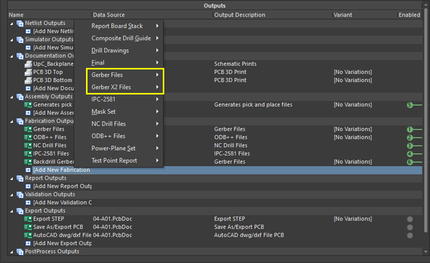
The first thing you should do is introduce a new OutJob template to your circuit board project. Upon adding the file, you can think of the manufacturing documents you must create and their formats.
As an illustration of these points, you can refer to the diagram below. It is a demonstration of several alternatives powered for various manufacturing documents.
We have chosen Gerber RS-274X documents and specifications for all back-drilled layers.
To generate a new export alternative for Gerber X2 templates, right-click the Fabrication Outputs button and choose the Gerber X2 item.
Source: https://resources.altium.com/p/generate-gerber-files-altium-designer-step-step-schematic-pcb
Remember that you can generate different sets of Gerber Outputs.
The diagram above shows the Backdrill Gerbers and the Gerber Files items on the RS-274X documents.
However, they will produce Gerber files for different layers.
After creating a new Gerber Output alternative
You should configure the data you will export with these options.
The diagram below illustrates the dialog to help you choose units, template format, and export layers. To use the conference, right-click one of your Gerber file items and press Configure.

Source: https://resources.altium.com/p/generate-gerber-files-altium-designer-step-step-schematic-pcb
The above diagram illustrates the dialog you will get for the RS-274X document.
Nevertheless, you will find the same discussion using the X2 form. It is important to note that the conference contains two primary buttons:
- The Layers Tab. You can maneuver through the Layers Tab to choose your preferred layers for export. They include electrical, mechanical, and silkscreen layers.
- The Drill Drawing Tab. If you had this button to choose the matching drill layers, you would adapt to a Gerber template. Naturally, this tab contains a top and bottom layer. But if you have powered any other Viator drill element, such as blind Vias, you will access their corresponding options.
In the diagram below, we have enabled all the Gerber templates and other manufacturing documents you should export.
To complete this process, hit the Generate Content button on the right side of your workspace.

Source: https://resources.altium.com/p/generate-gerber-files-altium-designer-step-step-schematic-pcb
Wow, you have successfully generated your Gerber files. As a professional, check your Gerber files to ensure they work correctly.
Remember, even simple issues can result in an unsuccessful fabrication run.
Watch the video below for a visual illustration of generating Gerber files in Altium Designer.
https://www.youtube.com/watch?v=qHFdHfF59hs
Eagle- Eagle Gerber Files
The critical point you should remember in Eagle Gerber files is that using Eagle templates for circuit board manufacturing is impossible.
Therefore, you should export your Gerber templates directly to a circuit board fabrication.
In this section, you will learn how to send Gerber documents from the Eagle .brd file to your PCB manufacturer.
Before creating Gerber files, the first thing to remember is to check whether the silkscreen lies on a single or double side.
This is because, by default, you will only generate the upper silkscreen layer.
Therefore, if your circuit board contains a two-sided silkscreen, you should also introduce the lower layer.
If your .brd file has milling designs, incorporate an additional outline layer before ticking the milling dimension.
Now, follow these steps to generate Gerber files for your PCB manufacturing.
Generate Drill Files
Running the drilling command is the first step in generating Gerber files in Eagle.
To achieve this, navigate to the File section and click Run ULP. Press OK on the pop-up that appears to create the conforming drill configuration template.
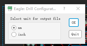
Source: https://www.autodesk.com/free-trials
Next, open the .brd document and scroll down the File section to open the CAM Processor.
Within the CAM processor, navigate to the File tab and click Open Access to the Open CAM Job. After that, press the Open tab in the excellent one. Cam dialog box.
Then, press the Process Job tab to create the conforming drill file.
Source: https://www.autodesk.com/free-trials
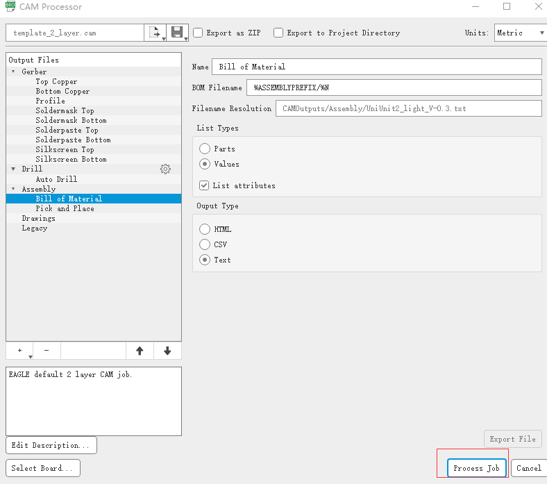
Generate Gerber Files
Remember, we are still in the CAM Processor dialog panel. Now proceed to the File section, select Open and click the Job button to access the Open CAM Job command.
Then hit the Open tab in the gerb274x. Cam section. Press the Process Job button when ready to create the matching Gerber template.
Source: https://www.autodesk.com/free-trials
Afterward, go to the panel labeled Add to modify these parameters: Change Section to Silkscreen b1, and File to %N.pls.
Additionally, discard the layers to remain with layers 20 Dimension, 22 places, and 26 blames.
If you encounter a milling design, remember to include an additional layer before selecting the 20 Dimension and 46 Milling.
Before sending your Gerber files to your PCB manufacturer, confirm that the layers are OK.
Compress your files in a .zip File.
The last step is compressing your files into one .zip file. Remember to fill out the circuit board document parameters before sending your Gerber file to your manufacturer.
Check out this link for a visual illustration of exporting Gerber files in Eagle.
https://www.youtube.com/watch?v=eBwfRZkkPII&t=19s
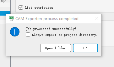
Eagle has made it easier for users to generate Gerber files in version 9.6.2. You only need to click the Process Job button to have your Gerber files.
The Importance of Gerber Files in PCB Manufacturing
Gerber files have increased functionality, including more configuration data and macro and aperture descriptions.
The laser plotters PCB manufacturers rely on today still utilize the same Gerber data. However, the aperture limitations of the earlier vector plotters are no longer applicable.
The plotters change the Gerber parameters to a raster document, as the data directs the plotter on how, where, and what to generate.
While the Gerber file sector continuously evolves, it will continue to hang on to its current state for a while before undergoing significant changes.
PCB Gerber Standard File Extension
| File Extension | Description |
| .GBR or.GER | Lists the PCB layer data, which includes copper traces, silkscreen layers, drill holes, etc. |
| .TOP and . BOT | Differentiates between the PCB’s upper and lower layers |
| .CMP | Shows the board design’s top layer components |
| .PLC | Indicates the component placement in the board design’s top layer |
| .SMT and . SMB | Shows the solder mask in the upper and lower layers, respectively |
| .SOL | Indicates the bottom-layer copper traces |
| .STC and . STS | Show the solder stencil information for stencil printing in the upper and lower layers, respectively |
| .DRD | Lists the drill data, including the hole location on the board. |
| .PHO | Used for photoplotter output files with the same data as Gerber files |
You can further detail the PCB layer data into Gerber files with the following extensions.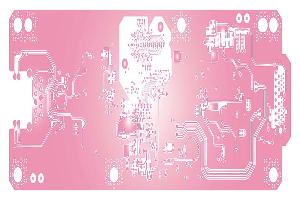
A pink layout of a PCB with the Gerber file of the inner layers
| .GTL | Indicates the top-layer copper pads and traces |
| .GBL | Lists the bottom-layer copper pads and traces |
| .GTS | Upper layer solder mask’s shape |
| .GBS | Contains the bottom-layer solder mask’s shape |
| .GTO | Top layer silkscreen information |
| .GBO | Lower layer silkscreen information |
| .GTP | Solder paste location on the upper layer |
| .GBP | Solder paste location on the lower layer |
| .GML | Mechanical layer (drill holes, non-copper features, PCB cutouts, etc.) |
| .GKO | Details the keep-out layer, where you cannot place traces or components |
| .G1 - .Gx | Lists the additional copper layers in multilayer boards |
| .GP1 - .GPx | Indicates the additional internal plane layers in multilayer PCBs |
How to Open GBX Files
There are five simple steps for opening a GBX file:
First, double-click the GBX file icon. If it fails to open or an error message pops up, proceed to the next step.
Secondly, select the appropriate program. If your file fails to open in step one, your computer lacks some basic GBX programs. Download some GBX programs to sort out the issue.
Thirdly, figure out your file types.
Next, contact your developer if you are still experiencing problems opening your GBX template.
Lastly, install a universal file viewer if the problem persists. You can still use it to open numerous types of files.
Conclusion
As a PCB designer or a fabrication engineer, you should master circuit board manufacturing requirements to generate Gerber files properly.
Some manufacturers request two aperture lists and additional data templates.
Therefore, you should understand the role of those templates and how to generate them.
While most PCB processes are automated nowadays, it is still essential to understand the Gerber file generation process and the whole PCB design process.
Special Offer: Get $100 off your order!
Email sales@ourpcb.net to get started!