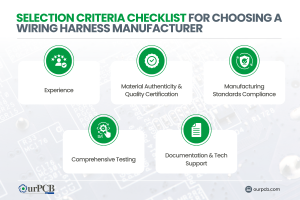
Top 10 Classic Car Wiring Harness Manufacturers | Full Guide
Finding the right wiring harness manufacturer for your vintage ride can be a real headache. Those beautiful old machines need special wiring that looks period-correct

OurPCB is a PCB manufacturer for hobbyists. We make custom circuit boards for DIY projects. Our focus is on small-batch production and prototypes, and we offer high-quality fabrication with quick turnaround times. OurPCB aims to support the creative needs of electronics enthusiasts.


Hobby PCB fabrication is the process of making custom circuit boards for personal projects. It involves etching copper traces onto a board to create electrical connections, which allows hobbyists to bring their electronic designs to life. The process starts with a design file, often created using software like KiCad.
We use advanced techniques to produce accurate, reliable PCBs for hobbyists. Our equipment can handle complex designs with fine details. We offer options like different board materials and finishes that meet your specifications. Our goal is to provide professional-grade fabrication for personal projects. We support both through-hole and surface-mount components.


Partnering with OurPCB for your hobby circuit boards offers many advantages, from quality assurance to flexible options. We understand the unique needs of hobbyists and DIY enthusiasts. Our services are tailored to support your creative projects. Here are the key benefits:

Hobby PCB manufacturing allows you to create custom boards for your projects. It gives you control over your design and components, which is ideal for unique or small-scale electronic projects. Here’s why you should consider it:

We offer comprehensive PCB assembly services to complement our fabrication options. Our assembly process ensures your boards are ready for use. We can handle various component types and board complexities. Here’s an overview of our assembly services:
Our technical capabilities cover a wide range of PCB manufacturing needs. We can produce boards with features as small as 2.5 mil traces and spaces, while our vias can be as small as 0.1 mm in diameter. We offer various surface finishes, including ENIG and lead-free HASL. Our equipment can handle up to 50 layers of board for complex designs, and we provide options for flexible and rigid-flex PCBs.
Mon-Fri: 24 hours,
Sat: 9am-6pm, GMT+8
Reach us at
[email protected]
24 hours online
+86-199-30589219
Mon-Fri: 24 hours,
Sat: 9am-6pm, GMT+8
To manufacture a PCB at home, design the printed circuit board layout, export Gerber files, and use an online PCB service or DIY etching. Apply a solder mask to protect traces, then drill and solder components. Many in the hardware community use OSH tools for open hardware projects. PCB fabrication and assembly at home is ideal for a PCB prototype.
PCB thickness options vary by design, with common choices from 0.4 mm to 2.0 mm. Figured it’s best to match thickness with application needs for durability. Manufacturers and online PCB services provide custom thickness options. Thickness impacts flexibility, weight, and heat dissipation.
To trace a PCB, follow signal paths on the printed circuit board using software. Analyzing Gerber files helps understand connections for debugging or cloning. DIYers and the hardware community use OSH tools for this. PCB fabrication and assembly insights improve troubleshooting.
Finding the right wiring harness manufacturer for your vintage ride can be a real headache. Those beautiful old machines need special wiring that looks period-correct
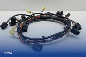
Would your car be able to run without wire harnesses? Not a chance. Wire harnesses connect all the electrical parts together. No harness means no
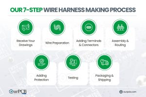
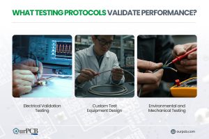
Making wire harnesses isn’t complicated. At OurPCB, we create custom wire harnesses for an expansive range of industries every day. While it’s a complicated process,
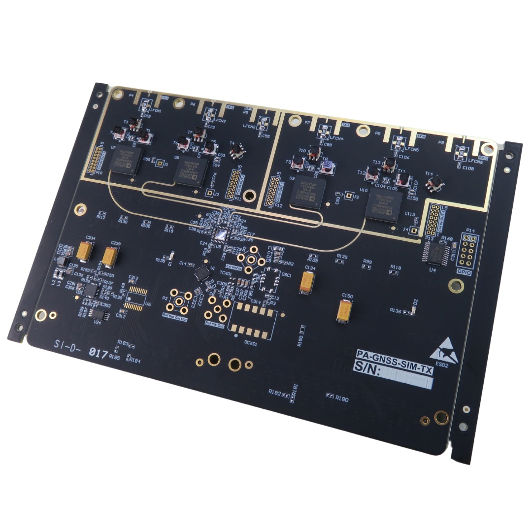
Prototype cable assemblies are the very important place in between PCB design ideas and interconnects. OurPCB brings prototype assemblies with PCB solutions to your tables.
PCB thermal management prevents component overheating through strategic heat transfer techniques. Without proper thermal control, electronics are at risk of electronic failures through weakened solder
ContentsKey TakeawaysWhat is a Multilayer-Printed Circuit Board?How do Multilayer PCB Boards Work?Multilayer PCB ApplicationsMultilayer PCB Manufacturing Process: StepsMultilayer PCB Manufacturing MachinesBenefits of Multilayer Circuit BoardsWhat
We use cookies to improve your browsing experience, which may include personal information. By clicking "Agree," you accept our Privacy Policy and cookie use. You can change your cookie settings in your browser anytime.
Agree
 Chat With Us
 Free Quote