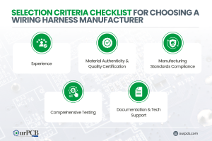
Top 10 Classic Car Wiring Harness Manufacturers | Full Guide
Finding the right wiring harness manufacturer for your vintage ride can be a real headache. Those beautiful old machines need special wiring that looks period-correct

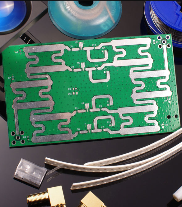
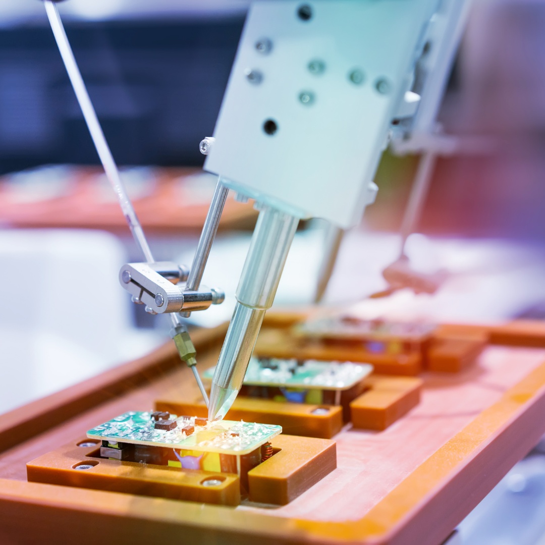
OurPCB, a high frequency PCB manufacturer, delivers advanced circuit boards designed for signal transmission above 500 MHz. Alongside fabrication, we provide complete circuit board assembly solutions to ensure your designs move smoothly from prototype to production. We offer custom RF and microwave PCBs using materials such as Rogers, PTFE, and ceramic-filled laminates. Our production ensures tight impedance control, low signal loss, and consistent performance for 5G, radar, and aerospace applications.


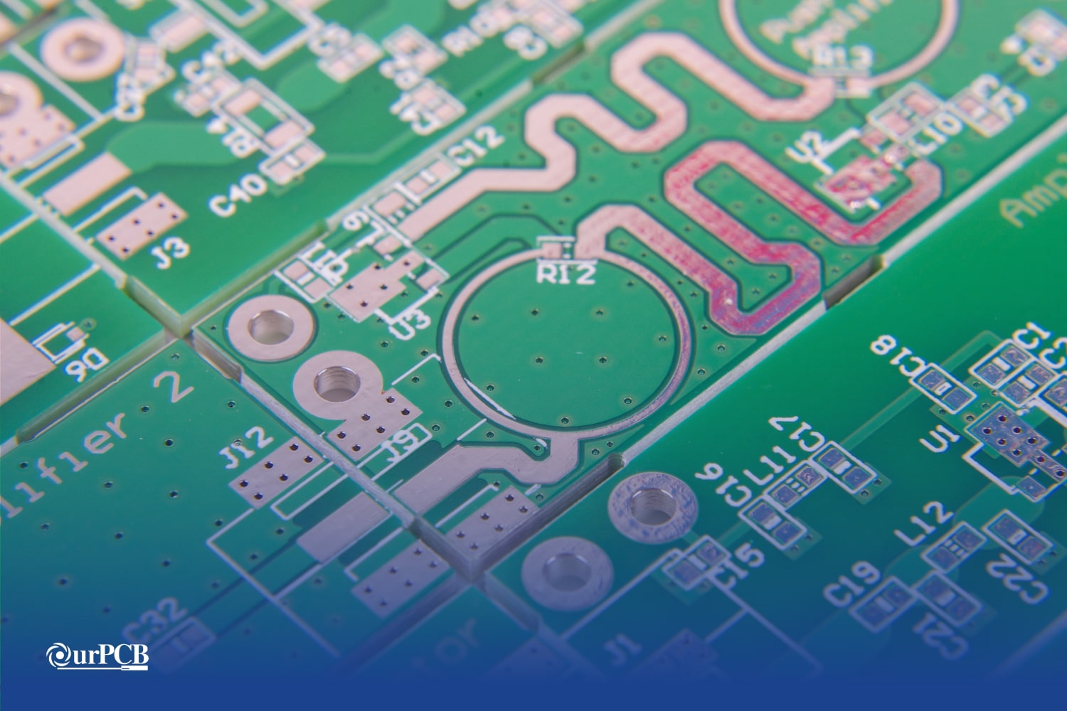

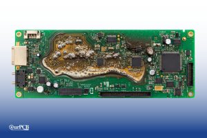
High-frequency printed circuit boards (PCB) are specifically designed to operate at high frequencies. A high-frequency PCB design makes it easy to achieve fast data transmission and improved signal integrity. There is a much higher demand these days for high-speed communication and wireless technologies, so as a high speed PCB manufacturer, it’s important to understand the ins and outs of high-frequency PCBs.


The PCB materials used in a high-frequency printed circuit board must have very specific electrical and mechanical properties. In some designs, advanced finishes such as the Selective Gold Plating Process are applied to enhance conductivity and prevent oxidation in high-reliability applications. This is to make sure that the high-frequency board performs well at higher frequencies. Here are some of the most common materials used.

Even though standard FR-4 is not ideal for high frequencies, specialized high-frequency versions with lower Dk and Df can definitely work.
Rogers Corporation makes a range of high-performance laminates like RO4350B and RT/duroid, which can provide powerful electrical properties for high-frequency PCB applications.
Taconic has materials like RF-35, TLY, and TLX, which are designed for high-frequency and microwave applications.
These materials can give you very low Dk and Df, making them great for extremely high-frequency applications.
These materials bring together the strong electrical properties of PTFE with a higher dimensional stability. An advanced ceramic substrate is usually used for applications that need powerful thermal stability and low signal loss.
LCP has fantastic electrical properties and can be used for both rigid and flexible high-frequency PCBs.
This material is popular because it has a high temperature resistance. Polyimide is used in high-frequency applications that need thermal stability.
Specialized prepreg materials can be used to bond layers in multilayer high-frequency PCBs while ensuring low signal loss.
High-frequency PCBs are incredibly unique in comparison to standard PCBs. Here are a few important properties that make them different:
These special properties allow radar PCBs to easily manage challenges with high-frequency and high-speed signals. They make sure that there is high reliability and powerful performance in the most demanding applications!
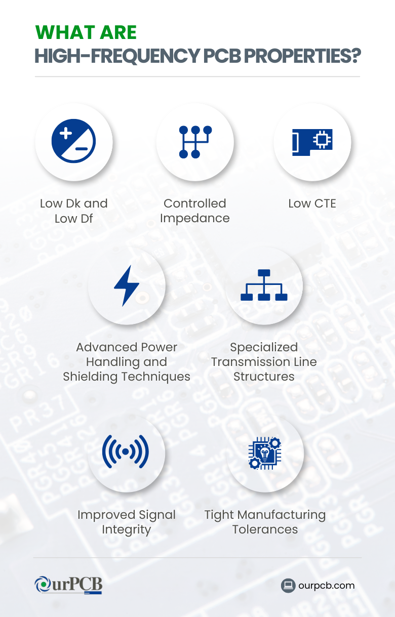
High-frequency PCBs come with tons of benefits that make them essential when it comes to modern electronics:
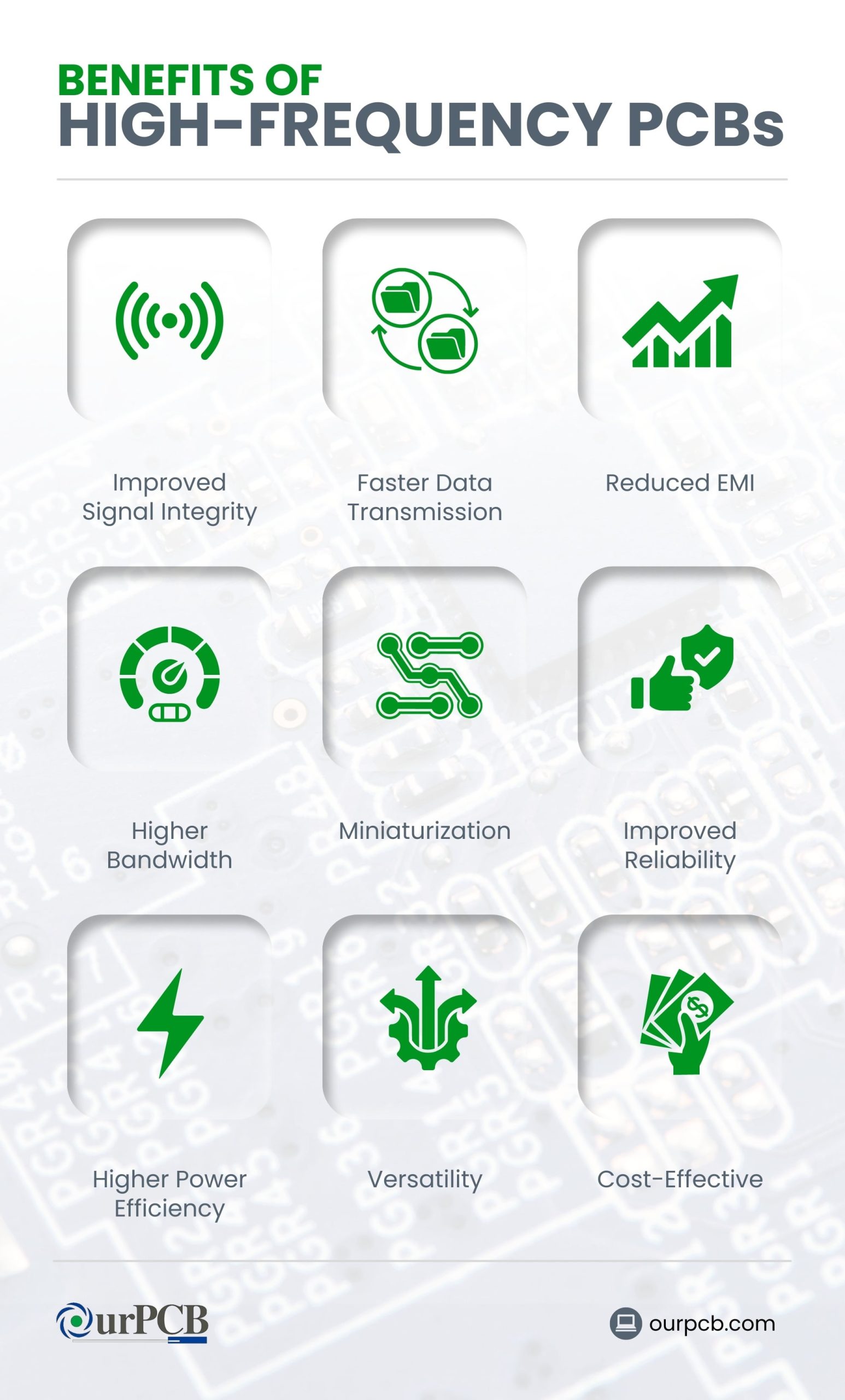
High-frequency PCBs maintain signal quality at high speeds. This reduces distortion and loss.
These PCBs allow for fast data transfer, which is essential for high-speed digital and wireless applications.
Proper design and materials help reduce EMI, which improves the overall system performance.
High-frequency PCBs can support wider frequency ranges, which means an increased data capacity.
Advanced designs allow smaller form factors without affecting performance.
Specialized materials and design techniques improve long-term reliability in high-pressure environments.
High-frequency PCBs can handle higher power densities with better thermal management.
These PCBs support tons of different applications, from consumer electronics to aerospace systems.
Even though these PCBs can be initially more expensive, they can lower the total system costs by improving performance and reliability.
We handle everything from parts sourcing to final assembly, providing a hassle-free experience that ensures top-quality boards every time.
Whether you need a few prototypes or large-volume batches, our flexible assembly services adapt to your project’s scope and timeline.
Stay environmentally responsible with our compliant assembly processes, offering RoHS and lead-free options for safe, reliable builds.
No matter the complexity, we can assemble boards of all configurations—single-layer, multi-layer, or a mix—to match your exact specifications.
From one-off prototypes to bulk orders, we accommodate projects of all sizes without compromising on quality or turnaround time.
Join our growing community of satisfied clients who rely on our dependable assembly expertise and dedicated customer support.
Mon-Fri: 24 hours,
Sat: 9am-6pm, GMT+8
Reach us at
[email protected]
24 hours online
+86-199-30589219
Mon-Fri: 24 hours,
Sat: 9am-6pm, GMT+8
The maximum high-frequency signals of a PCB can reach up to several hundred GHz in specialized applications; however, the majority of commercial high-frequency PCB applications typically operate in the range of a few GHz to tens of GHz. The maximum signal will also depend on the kind of materials and the design you use.
High-speed PCBs focus on fast digital signal transitions, whereas high-frequency circuits are designed for efficient analog or RF signal transmission at high frequencies.
High-frequency printed circuit boards (PCBs) are essential in any system that must reliably operate at radio-frequency (RF) and microwave frequencies. Typical applications include:
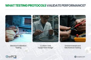
Designing high-frequency PCBs requires careful attention to materials, layout, and signal integrity. Follow these steps:
Yes. As a bare PCB board wholesale factory, we can fabricate high-frequency PCB substrates without assembly for clients who prefer to handle their own component sourcing and population. This option is ideal for large-scale production houses and specialized RF engineering firms.
Absolutely. Understanding how 7 segment displays work is important when designing control circuitry. High-frequency PCBs can be engineered to handle both RF signal processing and driving visual indicators, which is useful in test equipment, communication panels, and industrial monitoring systems.
Finding the right wiring harness manufacturer for your vintage ride can be a real headache. Those beautiful old machines need special wiring that looks period-correct
Would your car be able to run without wire harnesses? Not a chance. Wire harnesses connect all the electrical parts together. No harness means no
Making wire harnesses isn’t complicated. At OurPCB, we create custom wire harnesses for an expansive range of industries every day. While it’s a complicated process,
Prototype cable assemblies are the very important place in between PCB design ideas and interconnects. OurPCB brings prototype assemblies with PCB solutions to your tables.
PCB thermal management prevents component overheating through strategic heat transfer techniques. Without proper thermal control, electronics are at risk of electronic failures through weakened solder
ContentsKey TakeawaysWhat is a Multilayer-Printed Circuit Board?How do Multilayer PCB Boards Work?Multilayer PCB ApplicationsMultilayer PCB Manufacturing Process: StepsMultilayer PCB Manufacturing MachinesBenefits of Multilayer Circuit BoardsWhat
We use cookies to improve your browsing experience, which may include personal information. By clicking "Agree," you accept our Privacy Policy and cookie use. You can change your cookie settings in your browser anytime.
Agree
 Chat With Us
 Free Quote