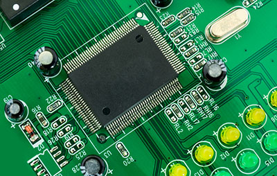
Altium Designer is irrefutably one of the commonest sophisticated Printed Circuit Board (PCB) design tools in the engineering market currently. It is built and supplied by Altium Limited, Above all, it and it comes with several features, like a schematic and auto-router.
Altium Designer software comes with high-powered tools for performing various circuit design activities, such as Schematic, circuit circulation, PCB design, and others. Besides, you can customize the Altium Designer workspace to carry out various user requirements.
Welcome to this tutorial of PCB design and realization in Altium's high-end software package. The tutorial will help you break into the entire process of making a PCB- from setting up a design project to output documentation.
Contents
- What is Altium?
- Altium Designer Tutorial
- Step 1: Altium Designer Download
- Sign Up for a Free User Account on the Altium Website
- Login on Altium Website
- Run Altium Designer Installer
- License Altium Designer
- Step 2: Setting Up Your Design Project
- Creating a New PCB Project
- Adding a Schematic to the Project
- Setting the Document Options
- Components and Libraries in Altium Designer
- Accessing Components
- Making Libraries Available
- Step 3: Placing Components on the Schematic
- From the Libraries Window
- From the Explorer Window
- Multi-vibrator Components
- Step 4: Add PCB
- Wiring the Schematic
- Wiring Guide
- Nets and Net Labels
- Step 5: Compiling the Project to Check for Errors
- Step 6: Creating a New Circuit Board
- Transferring the Schematic to the PCB Editor
- Setting up the PCB Workspace
- Configuring the Display Layers
- Step 7: Output Documentation
- How to Prepare Several Outputs in an OutputJob
- How to Configure Gerber Files
- Configuring the Bill of Material (BOM)
- Generating the BOM
- Mapping Design Data into the BOM
- Conclusion
What is Altium?
To begin with, Altium is a unified PCB design software package that hosts numerous design tools under one roof. Altium Designer 20- the latest version of Altium- symbolizes many years of innovation and improvement devoted to building a truly integrated design tool. For this reason, it allows users to efficiently utilize all the features of the circuit board design process features.
Remarking the excellent balance between control and ease of application, Altium has emerged as one of the most popular PCB design tools. Altium developers have developed an intuitive interface, putting the power of the software at users' fingertips. Generally, Altium Designer supports PCB engineers to actualize their creativity.
The Altium Designer workspace comprises of two key components:
- The first one is the primary document editing environment of Altium Designer is located on the right side of the application.
- The second environment is the Workspace Panels. Altium docks some panels on the left side of the tool; Besides, some panels pop-out on the right-hand side, some float, and others are concealed.
Altium Designer Tutorial
In this subheading, you will learn how to download the Altium Designer software, set up the design project, and place components on the Schematic. At the same time, you will also learn how to add PCB, compile the project to check for errors, create a new PCB, and output documentation.
Step 1: Altium Designer Download
Learn how to download a free version of Altium Designer, install and license it on your computer by following these steps.
Sign Up for a Free User Account on the Altium Website
Before you begin the download process, you need to sign up for a free user account on the Altium website. Join the Altium community of engineers and designers through this link.
Login on Altium Website
After signing up with the Altium community, login to your account through this link. Have a closer look at the features and advantages of Altium Designer before you proceed to the next step.
After approving the components and benefits of Altium Designer, you can download the Altium software from the Download Page.
Run Altium Designer Installer
When you have finished downloading the Altium Designer software, you should run it on your computer by pressing the Yes button on the pop-up window. Consequently, you will see a page welcoming you to the Installer. Hit the Next button to continue.
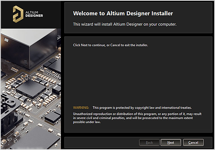
Source: https://www.altium.com/documentation/altium-designer/installing-altium-designer
Next, navigate to the Design Functionality to choose your preferred functionality and press the tab labeled Next.
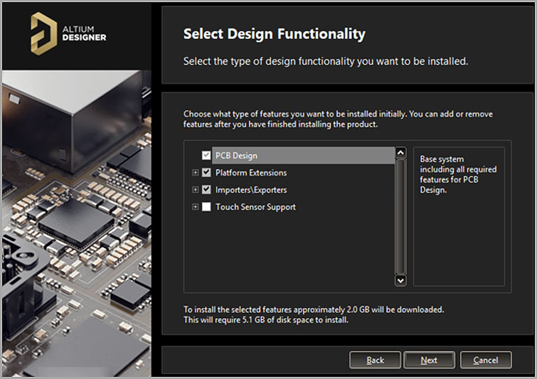
Source: https://www.altium.com/documentation/altium-designer/installing-altium-designer
Choose the computer folders where you will install your download and hit the Next tab.
After some time, depending on your internet speed, a Complete Installation panel will pop-up.
Congratulations! You have successfully finished the download and installation process. Tick the Run Altium Designer box and press the Finish button to close the Altium Installer.
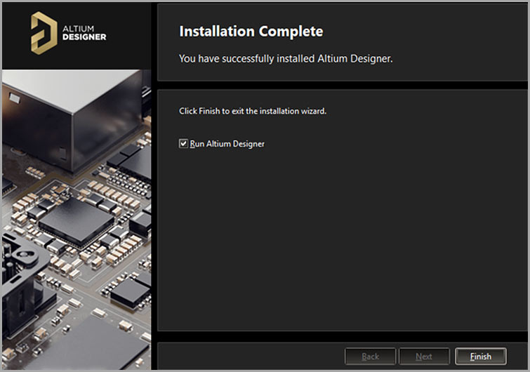
Source: https://www.altium.com/documentation/altium-designer/installing-altium-designer
License Altium Designer
If it is your first time to run Altium Designers on your device, a License Management Panel will show up, implying that you are using an invalid license. Sign in to your Altium account that you created earlier to access a list of valid permissions.
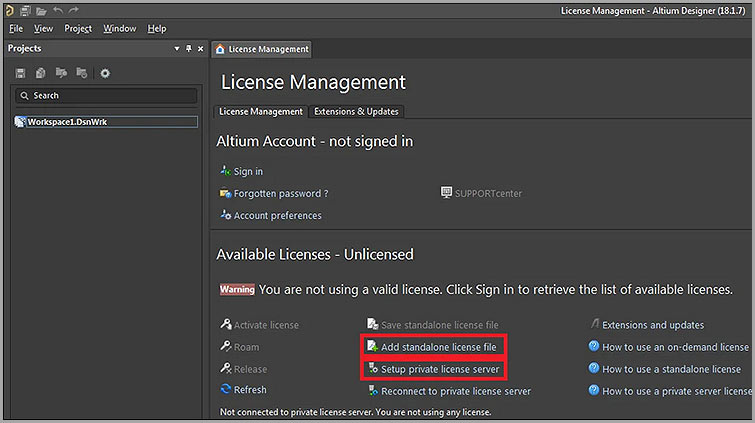
Source: https://www.altium.com/documentation/altium-designer/installing-altium-designer
Step 2: Setting Up Your Design Project
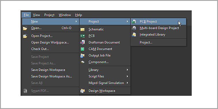
Creating a New PCB Project
According to Altium Designer developers, a PCB project is a set of design templates needed to specify and make a PCB. For instance, the project template, Multivibrator.prjPCB, is an ASCII template that stipulates all the project documents and project-based settings, like rule checks.
Now, you can create a new project through the File section, Select New Project, and click the PCB Project tab.
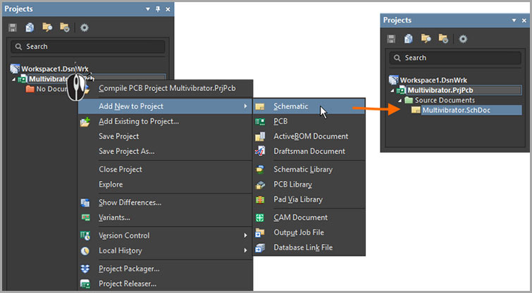
Adding a Schematic to the Project
For the purpose of the next steps, you need to add a schematic sheet to your project, as shown below.
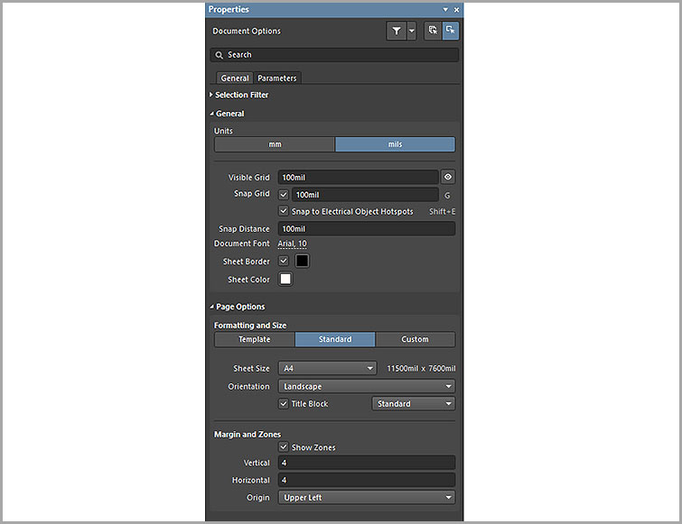
Setting the Document Options
In the first place, you should set up the right document options, such as the sheet size and Snap, before you begin drawing your PCB.
Components and Libraries in Altium Designer
The elements that you will add to the PCB appear as schematic symbols in the design capture process. You can either:
- Make components within and place from local libraries, or
- Access them through the Content Vault, all-round component storage containing numerous elements.
Accessing Components
You can access components via the:
- Libraries window in case of library components, or
- Explorer window in case of Content Vault components
- You can easily reach both windows through the Panels tab.
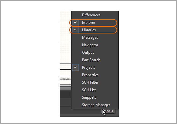
Making Libraries Available
Unlike other PCB design tools, you can place library components from existing libraries In Altium, such as:
Those in the current project- use the components of a library belonging to a particular project in any running project.
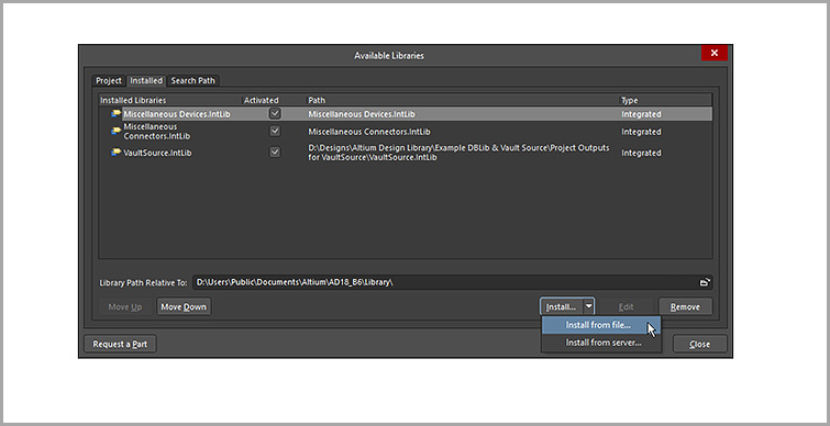
In this case, you should install the libraries in the Installed section within the Available Libraries panel. To access the dialog, hit the Libraries tab on the Libraries window. If you are unable to view the forum, navigate to the Panels, and click Libraries.
https://www.youtube.com/watch?v=NDtADnhvlDQ
Special Offer: Get $100 off your order!
Email [email protected] to get started!
Step 3: Placing Components on the Schematic
You can access components in the Libraries/, or Explorer window and place them on any running schematic.
From the Libraries Window
Using the Place tab- position and press to insert the component floating on your cursor. After placing it, right-click to leave the placement mode.
Double-clicking- by double-clicking the Components tab in the window's component section, you will see them floating on your cursor. You need to position it appropriately and press to insert it. Then right-click to leave the placement mode.
Clicking and dragging- you can also place components on the Schematic from the Libraries panel by clicking and dragging the Schematic element. However, you should hold your cursor down and release it to put your component.
From the Explorer Window
Right-click the component and choose Place to float it on your cursor. Then position it appropriately and press to insert. When the Explorer window floats on your workspace, it will quickly fade to enable you to view the schematic drop components. Right-click to leave the placement status.
Click and drag- You can also click and remove parts from the Explorer window and place them on the Schematic. You should hold your cursor down and release it to set the component. Based on your internet speed, you might experience a short delay before placing the parts.
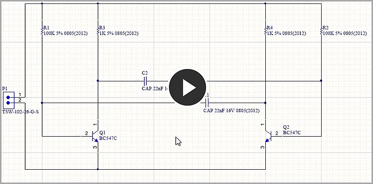
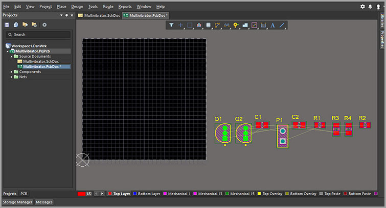
Multi-vibrator Components
Navigate to the Content Vault to check these designators: Q1, Q2, R1, R2, R3, R4, C1, C2, and P1. Place them to create a schematic similar to the diagram below.
Remember, the collapsible parts comprise tips on designing the placement process, which is more effective than developing after placement.
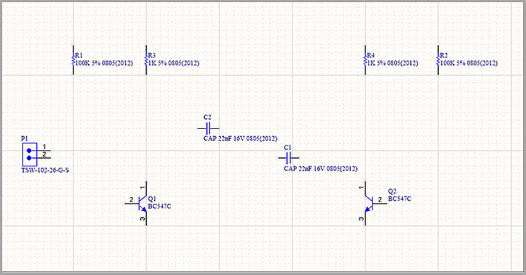
Congratulations! You have successfully positioned the components. However, you should widely space the components as illustrated above to create enough space for wiring all the component pins. You require adequate spacing since you cannot position wires underneath pins to access them beyond the wires. Otherwise, you will link all the pins to the wire. When moving components, press-and-hold them and relocate them by dragging the mouse.
Step 4: Add PCB
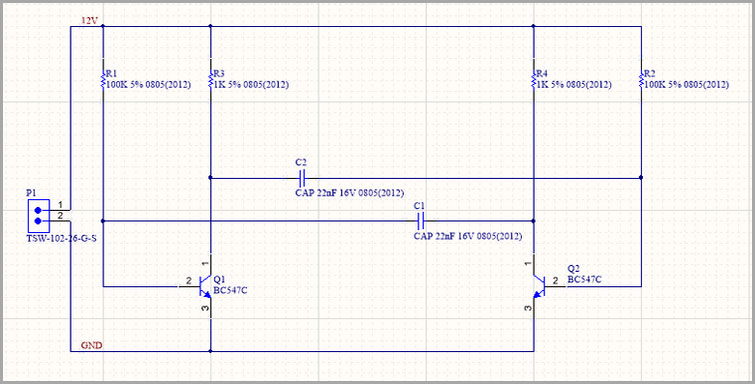
Wiring the Schematic
The first thing to do in adding a PCB is to wiring your board to create connectivity between the different parts. Luckily, the wiring process is easy. As an illustration, refer to the diagram below.
Wiring Guide
First, left-click or use the Enter bar to tie up your wire at the cursor point.
Secondly, use the Backspace to delete the previous anchor location.
Thirdly, use the Spacebar to clip the bearing of the junction.
Fourthly, hold the Shift and Spacebar to rotate through the wiring junction modes.
Next, Right-click to leave the wire posting mode. Alternatively, you can use the ESC tab.
Then Finally, press and hold to relocate positioned components. You can also press ctrl, click, and hold at the same time to move the parts together with the wires.
If any wire crosses a link of any part, you will end up creating a junction.
Nets and Net Labels
Every set of arts that you have linked is known as a net. For instance, a net can consist of base Q1, pin R1, and C1. Altium naturally assigns every net a label based on the type of component pins.
You can introduce Net Labels to assign labels and simplify the identification of basic nets.
Name 12v and GND nets in the multi-vibrator circuit.
Step 5: Compiling the Project to Check for Errors
To assemble your project, examine inaccuracies, navigate the Project section, and select Compile PCB Project Multi-vibrator.prjPCB.
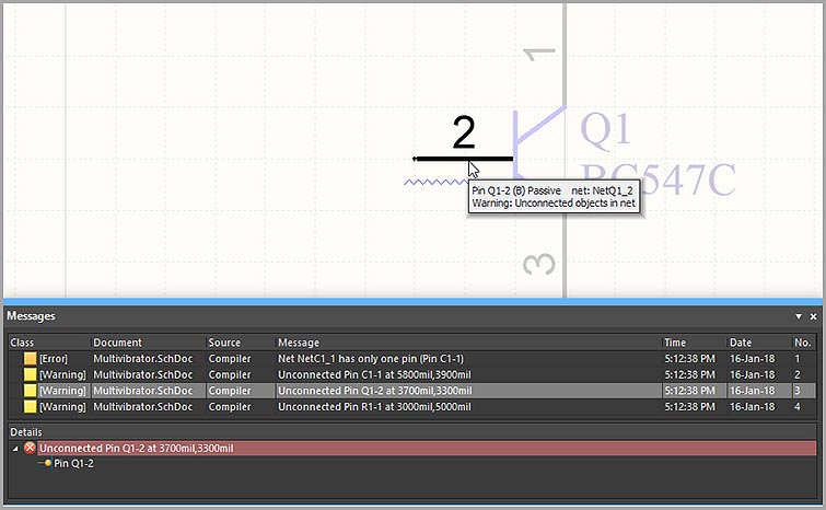
Wow, your Schematic is now fully complete!
Step 6: Creating a New Circuit Board
Before you relocate your schematic design to the circuit board editor, you should make a blank PCB, label, and save it.
There are several settings of the blank PCB that you need to modify before moving your schematic design. They include defining the origin, changing the imperial units to metric, choosing an appropriate snap grid, resizing the PCB shape to the recommended size, and arranging the design layers.
Click Ctrl and PgDn anytime you want to zoom and view the whole circuit.
The best way to delimit the shape of a non-rectangular PCB is by placing tracks on the keep-out layer.
Transferring the Schematic to the PCB Editor
It would be best to move your Schematic directly from the schematic editor to the circuit board editor. You do not have to create another netlist document to facilitate the transfer.
First, proceed to the Design section of your schematic editor, and click on Update PCB Document Multi-vibrator.PcbDoc. Alternatively, you can go to the circuit board editor and click on Design, then choose Import Changes Multi-vibrator.PrjPcb.
If you use one of the above commands, you will compile your design and generate some orders, like:
List every schematic component and its corresponding footprints. When you implement the ECOs, the application will try to find each impression in the libraries or Content Vault and position them in the workspace's circuit board.
The software generates a list of schematic nets. It would help if you implemented the ECOs to relocate the nets to the circuit board and introduce every net's pins.
You can then transfer extra schematic data, like component classes.
Setting up the PCB Workspace
Once you have completed all the ECOs, parts and nets will pop-up on the right side of your circuit board workspace, as illustrated below.
Before placing the parts on the PCB, you should modify the board working area and some settings, like layers and grids.
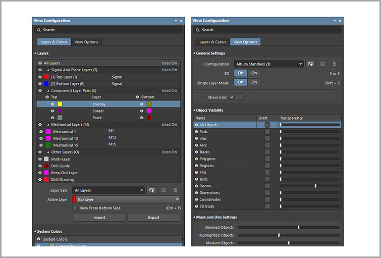
Configuring the Display Layers
Apart from the PCB fabrication layers, the circuit editor also facilitates other non-electrical layers. These layers are mostly classified, as shown below:
Electrical layers, like the 32 signal layers.
Mechanical layers, like the 32 general use mechanical layers, which are useful in design activities and special purpose activities. They can also be used in the print and Gerber generation or paired.
Another standard layer is the unique layers, such as the upper and lower silkscreen layers and the multi-layers.
The View Configuration window configures the display characteristics of each layer. To access it:
Go to the Panels section at the lower side of your workspace and click View Configuration, or
Navigate to the View bar, choose the Panels option and click the View Configuration tab, or
Use the L alternative, or
Press the existing color layer tab at the lower left side of the application.
Step 7: Output Documentation
Since you have finished designing and laying your board, you should proceed to create the output documentation, which is useful in reviewing, fabricating, and assembling the PCB.
There are several circuit board manufacturing methods, and luckily, Altium Designer can create various outputs for a wide range of purposes.
The first category is assembly output, comprising assembly drawings and pick & place documents. The second category is documentation outputs, consisting of PCB prints, PCB 3D prints, PCB 3D video, PDF3D, and schematic prints.
The third category of outputs is known as fabrication outputs, and it comprises Gerber files, IPC-2581 template, ODB++, drill drawings, and others.
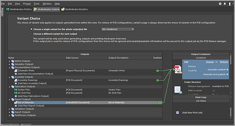
How to Prepare Several Outputs in an OutputJob
There are two methods of configuring and creating outputs in Altium software:
Individually. Here, you keep the configurations of each output in the Project template. Go to the Fabrication Outputs, select the Assembly Outputs, click the Export tab, and press the Reports button to create an individual output.
Through an Output Job Template- after keeping the configuration of all outputs in the Output Job document, you can create the outputs manually.
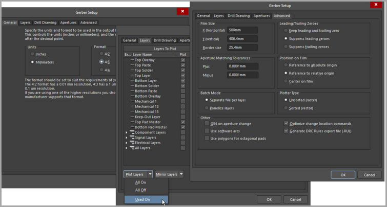
How to Configure Gerber Files
Gerber is commonly used to move data from PCB design to fabrication. Every Gerber document matches a particular layer in the physical PCB.
It would help if you referred to your PCB supplier to check their terms and conditions before making the fabrication process' output templates.
Remember, if your PCB contains holes, you should create the NC Drill template with the same measurements, resolution, location, and onboard configurations.
You can configure Gerber templates within the Gerber Setup panel, accessed through the board editor. Go to the Fabrication Outputs and click the Gerber Files.
Configuring the Bill of Material (BOM)
Altium Designers contains a management editor ActiveBOM that you can:
- Use to configure the component data and make it ready for the Bill of Material.
- You can also include extra non-PCB features, like the mounting hardware.
Use them to introduce more columns to meet the demands of the assembly workspace.
For this reason, map every design part of its corresponding supplier component.
Then, authenticate the supply and price of any component for a certain number of produced units.
Lastly, estimate the cost to create a given number of produced parts.
Generating the BOM
To develop a BOM output, go to the Reports panel in your circuit editor and click on the Materials Bill. Alternatively, you can introduce the BOM to your Report Outputs panel
Mapping Design Data into the BOM
Remember, you need to transfer the design information from the application into an Excel BOM You can achieve this by inserting special commands in the Excel document used to build the Bill of Materials.
When you are making the BOM file in Excel, you can utilize both Fields and Columns to stipulate the right layout. Altium software contains various files within the /Templates section.
Conclusion
In reality, PCB design is not a walk in the park and very few design software come with the right tools to make your project a success. Luckily, Altium Designers has a simple and intuitive user interface.
We created this Altium Designer Tutorial to help you break into the entire process of making a PCB- from setting up a design project to output documentation. In your PCB designing ventures, consider using a PCB software that integrates and builds consistencies between steps quickly, like Altium Designer.
Most powerful and cutting-edge board design tools are expensive.
However, Altium developers have come up with CicuitMaker- a board design application with free access to the features, that enable PCB designers to actualize their creativity without limitations.
You can try this free version before purchasing one.
Special Offer: Get $100 off your order!
Email [email protected] to get started!