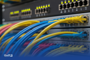
Who are the Top 6 Data Cable Manufacturers in China?
When considering the best places for manufacturing data cables, China immediately comes to mind. It’s no surprise either — the country has rapidly ascended in

Looking for a reliable PCB manufacturer of Flexible or Rigid-Flex PCBs? OurPCB provides high-quality, custom-designed solutions for OEMs with fast turnaround times to the USA and worldwide. We serve industries including automotive, medical devices, consumer electronics, and more.


Below is a detailed overview of our Flex & Rigid-Flex PCB capabilities, showcasing the key specifications and performance metrics that highlight our commitment to precision and quality in every project.
| Project Item | Normal Capability |
|---|---|
| FPC Base Material (Adhesive) | ShengyiSF302:PI=0.5 mil,1 mil,2 mil;Cu=0.5 oz,1 oz ShengyiSF305:PI=0.5 mil,1 mil,2 mil;Cu=0.33 oz,0.5 oz,1 oz |
| FPC Base Material (Adhesiveless) | SongxiaRF-775/777:PI=1 mil,2 mil,3 mil;Cu=0.5 oz, 1 oz (Ultimate:PI=1 mil,2 mil,3 mil;Cu=2 oz) Xinyang:PI=1 mil, 2 mil;Cu=0.33 oz, 0.5 oz, 1 oz Taihong PI=1 mil, 2 mil;Cu=0.33 oz, 0.5 oz, 1 oz Dubang AP:PI=1 mil, 2 mil, 3 mil, 4 mil;Cu=0.5 oz, 1 oz (Ultimate:PI=1 mil,2 mil,3 mil,4 mil;Cu=2 oz) |
| Layer | 1-6 Layers (Ultimate:7-10 Layers) |
| Thickness of Finished Product (Flex part,no stiffener) | 0.05-0.5 mm (Ultimate: 0.5- 0.8 mm) |
| Size of Finished Products(Min) | 5 mm*10 mm (Bridgeless);10 mm*10 mm (Bridge) Ultimate:4 mm*8 mm (Bridgeless);8 mm*8 mm (Bridge) |
| Size of Finished Products (Max) | 9 inch*14 inch Ultimate:9 inch*23 inch (PI≥1 mil) |
| Impedance Tolerance | Single-Ended:±5Ω(≤50Ω),±10%(>50Ω) Ultimate:Single-Ended:±3Ω(≤50Ω),±8%(>50Ω) |
| Impedance Tolerance | Differencial:±5Ω(≤50Ω),±10%(>50Ω) Ultimate:Differencial:±4Ω(≤50Ω),±8%(>50Ω) |
| Tolerance of Finger Width | ±0.1 mm (Ultimate:±0.05 mm) |
| Min Distance to the Edge of Finger | 8 mil (Ultimate:6 mil) |
| Min Distance between Pads | 4 mil (Ultimate:3 mil) |
| Minimum Laser Hole | 0.1mm |
| Minimum PTH | 0.3mm |
| Min NPTH Tolerance | ±2 mil (Ultimate +0,-2 mil or +2 mil,-0) |
| Solder Bridge Min Width(bottom copper<2OZ) | 4 mil(Green),8 mil |
| Solder Bridge Min Width(bottom copper 2-4OZ) | 6 mil,8 mil |
| Overlay Colour | White、Yellow (printed character:White) |
| Type of Surface Treatment | OSP HASL, Lead free HASL, Immersion gold, Hard gold, Immersion silver, OSP |
| Selective Surface Treatment | ENIG+OSP,ENIG+G/F |
| Project Item | Normal Capability |
|---|---|
| FPC Base Material (Adhesive) | Shengyi SF302, Shengyi SF305 |
| FPC Base Material(Adhesiveless) | Songxia RF-775/777, Xinyang, Dubang AP |
| Low flow prepreg | Taiguang EM-37B; Ventec: VT-47N |
| Common rigid board material | Refer to standard rigid board materials |
| Special rigid board material | Arlon: 85N; Rogers: RO4000 series; Nelco: N4000-13 series; Ventec: VT-901 |
| Layer | 2-30 Layers; review required: ≥20 layers |
| Thickness of Finished Product | 0.3-4.0mm; review required: >3.0 mm |
| Size of Finished Products(Min) | 10mm*15mm (no internal positioning designs, panel size <50mm*50mm) |
| Size of Finished Products (Max) | 18inch*22inch; Ultimate:18inch*29inch |


On average, flexible PCBs can range from $0.50 to $5.00 per square inch for standard designs and materials. However, this cost is not fixed and can vary based on several factors. The factors that influence the price include necessary assembly labor, prevailing labor rates, and the time required for assembly. Additionally, overhead manufacturing expenses and the design complexity of the board play significant roles in determining the final cost. To get a more accurate cost estimate, please use our free pcb quote form.

| Service Type | Lead Time |
|---|---|
| Standard PCB Manufacturing | 5-6 days |
| Expedited Manufacturing | 24-48 hours |
| PCB Prototyping (Quick Turn) | 1-12 layers: within 72 hours |
| 12+ layers: within 120 hours | |
| PCB Assembly | 4-25 days, depending on complexity and order volume |
China’s flex PCB industry offers many advantages, such as the combination of high quality with cost-effectiveness. Chinese manufacturers like OurPCB use advanced tech and skilled labor.

Step 12: Singulation and packaging
OurPCB offers flexible PCBs for innovative, space-saving designs. Starting at $172.50 for 5 units (1 layer, 100 mm x 100 mm), these PCBs are ideal for applications requiring flexibility and precision.
Mon-Fri: 24 hours,
Sat: 9am-6pm, GMT+8
Reach us at
[email protected]
24 hours online
+86-199-30589219
Mon-Fri: 24 hours,
Sat: 9am-6pm, GMT+8
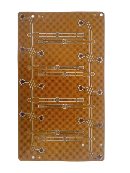
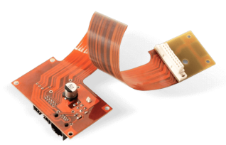
Flexible PCBs can be bent, shaped, wrapped, or folded into any 2D or 3D shape. These features make flexible PCBs perfect for use in medical and surgical equipment, consumer electronics, automotive and space applications, and smart wearable devices.
We have no minimum order quantity, allowing you to order anything from single prototypes to mass production runs.
Beyond manufacturing, we also provide full EMS: What is it? solutions – short for Electronics Manufacturing Services. That means we can take a project from the initial design concept, source every part you need, handle assembly and testing, and even package the finished boards so they’re ready to ship. For many clients, this “one-stop” approach is faster, more cost-effective, and removes the hassle of juggling multiple suppliers.
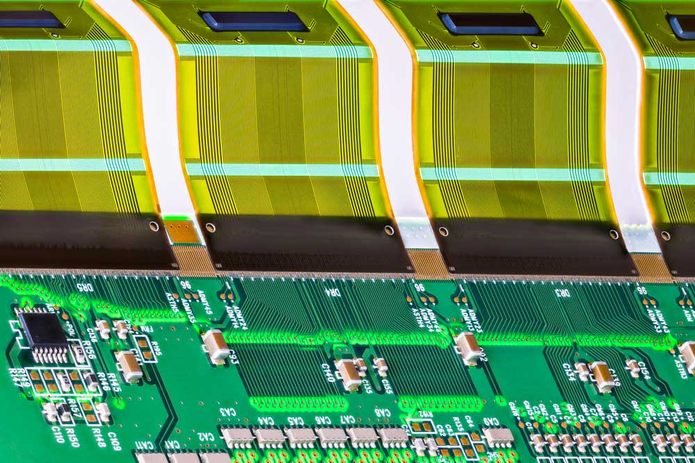
Absolutely. Our team works with High Density Interconnect PCBs for designs that require more circuitry in less space. With finer traces, microvias, and multiple build-up layers, HDI is often the right choice for rigid-flex PCBs in demanding fields like aerospace navigation, compact medical devices, and next-generation consumer electronics.
The overall flow follows the same core steps you’ll find in PCB Manufacturing Process Explained, but with important adjustments for flexible substrates like polyimide. For instance, we use different lamination techniques to maintain bendability, and our etching process is fine-tuned to protect thin copper layers from damage. Every stage is planned to balance flexibility with electrical reliability.
Before anything goes into production, our engineers and sourcing team go through a careful Identify Electronic Components process. We check each part against the project’s electrical, thermal, and mechanical requirements, and we confirm compatibility with the intended assembly method – something that’s especially important with flexible circuits.
We do. For example, in portable or sensitive electronics, overcurrent protection can make the difference between a safe shutdown and a burned-out circuit. In these cases, we’ll often recommend the use of the right Understanding Fast-Blow Fuses to provide rapid protection without impacting normal performance.
In short – experience and consistency. As a Reliable PCB Manufacturer, we’ve built long-term partnerships by delivering quality boards on schedule, communicating openly, and meeting industry certifications year after year. Many of our customers have been with us for over a decade.
One example is Troubleshooting Tombstoning in PCBs – a frustrating soldering defect where small passive components lift on one side during reflow. We address this through careful pad design, precise solder paste application, and temperature-controlled reflow profiles tailored to the flex board’s material properties.
Absolutely. Flexible PCBs are not just for industrial or aerospace applications — they’re perfect for compact, custom electronics as well. For example, our guide on Creating a 10 Minute Timer shows how even a simple timing circuit can benefit from a flex PCB layout, allowing it to fit into tight spaces while maintaining durability and performance.
When considering the best places for manufacturing data cables, China immediately comes to mind. It’s no surprise either — the country has rapidly ascended in
Finding the right wiring harness manufacturer for your vintage ride can be a real headache. Those beautiful old machines need special wiring that looks period-correct
Would your car be able to run without wire harnesses? Not a chance. Wire harnesses connect all the electrical parts together. No harness means no
Making wire harnesses isn’t complicated. At OurPCB, we create custom wire harnesses for an expansive range of industries every day. While it’s a complicated process,

Prototype cable assemblies are the very important place in between PCB design ideas and interconnects. OurPCB brings prototype assemblies with PCB solutions to your tables.
PCB thermal management prevents component overheating through strategic heat transfer techniques. Without proper thermal control, electronics are at risk of electronic failures through weakened solder
We use cookies to improve your browsing experience, which may include personal information. By clicking "Agree," you accept our Privacy Policy and cookie use. You can change your cookie settings in your browser anytime.
Agree
 Chat With Us
 Free Quote