As printed circuit boards become more complex, the impedance requirements for different traces or copper lines have increased. Therefore, you need stricter control over the width of the lines, which highlights the etching solution for PCB. PCB etching has and continues to evolve, and we will analyze the process and its types below. Take a look!
Contents
What is PCB Etching?
PCB etching is a process involving the removal of unwanted copper from the circuit board to create circuit patterns or copper traces. Before the etching process, manufacturers use the design file to define the board's circuit pattern layout. After that, they transfer this image to the PCB using a process known as photolithography. This image creates a blueprint to determine the areas in the copper layer that need etching and the ones that should remain on the board to form the patterns.
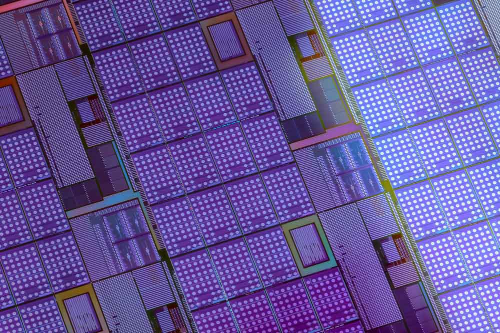
A monocrystalline silicon wafer with microchips after photolithography
Usually, manufacturers use tin plating to create this image (etch resist) on outer PCB layers to secure the copper areas that should not undergo etching. On the inner layers, they use photoresist as the etch-resist material.
There are two methods to eliminate the excess copper after placing these protective layers. They are dry and wet etching processes.
Special Offer: Get $100 off your order!
Email [email protected] to get started!
Dry Etching
The dry etching process does not use chemical solutions to dissolve copper. It creates plasma (positively charged gas) in a vacuum to shave off the excess copper.
The process is more complex than wet etching and requires dedicated etching machines to eliminate the excess copper material. Also, it does not produce any residue, is more flexible, and can achieve more precise material removal directionally.
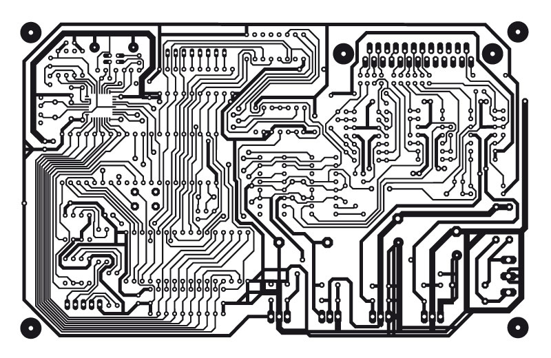
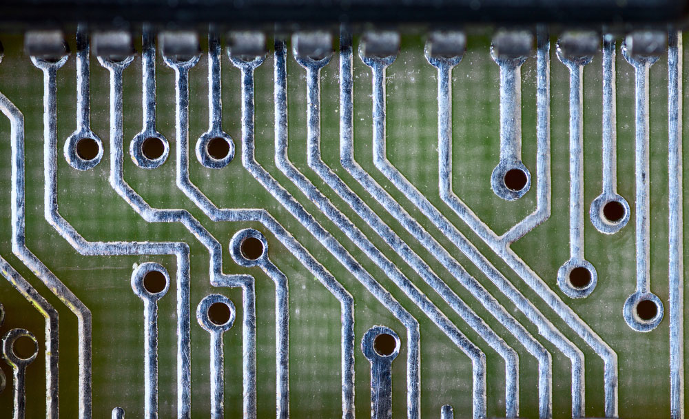
A PCB trace wiring design
More importantly, it is cleaner and requires less training, making it the preferred option for critical and agile manufacturing processes, such as those used in manufacturing microelectronics.
The most typical dry etching technique is Reactive Ion Etching (RIE).
Advantages of Dry Etching
- Environmentally friendly and safer
- Excellent at cleaning and removing organic materials on the copper surface
- Enhances the etched material's physical properties
- Creates volatile by-products
- It does not alter any property of the copper metal.
Wet Etching
Wet PCB etching involves immersing the PCB in a chemical solution to remove the unwanted copper. The PCB etching process can employ two methods depending on the PCB etching solution. They include acidic and alkaline methods.
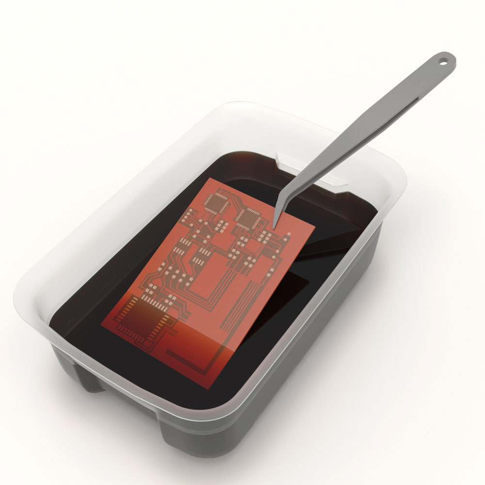
Chemical etching of a PCB
Acidic Etching
With the acidic method, fabricators use an acidic solution to etch the inner layers of rigid PCBs because it does not react with photoresist.
Compared to the alkaline etching method, acids do not create many undercuts. So the process is more precise. An undercut is a lateral erosion of the copper layer that occurs under the protective photoresist or tin material.
PCB etching using an acidic solution
Also, acidic etching is cheaper and does not corrode crucial sections on the circuit's blueprint. However, it is more time-consuming than its alkaline counterpart.
The solutions used for acidic etching include the following.
Etching Solution For PCB: Cupric Chloride
Cupric chloride is the most typical acidic etchant because it dissolves tiny features accurately. Additionally, the solution gives a constant etching rate and continuous regeneration at a lower cost.
Manufacturers can increase the etch rate of the cupric chloride solution by using a cupric chloride-HCl chloride sodium system. This combination increases the maximum etching rate of 55s for one ounce of copper at 1300°F.
PCB tracks up close
However, you must adhere to safety and emergency protocols when handling chlorine gas and should work in a well-ventilated room with cylinder storage, a tank, and leak-detection sensors.
Also, you will need personal protective equipment, approval from your area's fire department, and trained operators.
Etching Solution For PCB: Ferric Chloride
This solution has the following benefits as a commercial etchant.
- Easy to use
- High copper holding capacity
- Ideal for handling infrequent batches
However, it is not a common PCB etchant because of the high cost of disposing of the copper-saturated etchant as a hazardous waste product from the process.
PCB etching in a ferric chloride solution
Usually, manufacturers use it with photoresist, gold patterns, and screen ink because it is highly corrosive. Therefore, you cannot use the solution on tin or tin/lead resists.
In most cases, you must dissolve the ferric chloride solution in water to a concentration of 28-42% by weight. After that, add about 5% HCl to the mix to avoid the formation of insoluble ferric hydroxide precipitates. The final acid concentration for the solution used for commercial purposes is about 1.5-2%.
Alkaline Etching Process
The alkaline etching process uses only one chemical solution containing the following.
Chloride Copper + Hydrochloride + Water + Hydrogen Peroxide
This solution is highly corrosive, meaning it etches the board quickly and can damage it if you leave the PCB in the solution for a long time. Therefore, you must follow the parameters used in the process to the letter for precise control. And the procedure is expensive compared to acidic etching.
A photolithography slide for a semiconductor crystal
How Alkaline Etching Occurs
The process occurs in a high-pressure spray chamber with conveyors where the PCB gets exposed to a refreshed etchant spray. The following factors are crucial to creating uniform traces with minimal errors and straight sidewalls.
- Panels movement rate
- Etching chemical spray
- How much copper needs removal from the board
After eliminating every part of the excess copper, this alkaline etching process hits a point known as the breakpoint, where the procedure is complete. It usually occurs at the midpoint section through the conveyor spray chamber. For instance, if this chamber is one meter long, the breakpoint milestone will be at the 50 cm mark.
Parameters Defining the Quality of Etching Solutions For PCB
The following factors affect the etchant quality and smoothness of the wet etching process.
Temperature
High temperatures generally increase an etchant's etch rate, but the etching machine will constrain the achievable temperature. Most of these machines have plastic parts to avoid corrosion from the etchant chemical solutions. Therefore, the temperatures usually don't exceed 55°C to avoid melting these components.
Baume
Baume (Be) defines the molarity concentration in an etchant, and it depends on the solution's specific gravity. A high Be implies the solution has a high etchant molarity and dissolving rate. High Baume values also reduce undercuts.
Chemical Additives
Chemical additives increase the etch rate in commercial etching solutions. HCl is the most typical additive in acidic solutions because it acts as the source of chlorine to create metal chlorides instead of hydroxides.
The extra chlorine increases the solution's ability to hold the dissolved copper. You can introduce the additive to the acidic solution before first use or during regeneration, and you must measure the pH to check the solution's acidity before use.
The etching machine restricts the additives you can introduce to the solution because chlorine increases corrosiveness.
Oxidation-Reduction Potential (ORP)
The oxidation-reduction potential of an etchant is a measure of its relative conductivity in millivolts. This potential brings out the relationship between the following.
- Ferrous and ferric ions
- Cuprous and cupric ions
As the copper gets etched, the chemical solution changes from cupric or ferric to cuprous or ferrous. The higher the ORP value, the more efficient and faster the etchant operates.
Adding additives (free acids) and oxidizers to the solutions increases chlorine levels. The chlorine converts the cuprous and ferrous ions back to cupric and ferric ions, making the etchant more potent.
pH
The pH variable is crucial for alkaline etching because it should fall between 7.9 and 8.1 for reliable etching. Low pH levels below 8 are usually due to low ammonia, excessive ventilation, or heating.
And a high pH that exceeds 8.8 can be due to under ventilation, water in the etchant solution, or high copper content. Both these conditions reduce the etch rate.
With acid etching, high pH levels create incorrect copper colorimeter readings due to solution turbidity.
Advantages of Wet Etching
- Cheaper than dry etching
- Creates a uniform surface
- More adaptable
- Offers impeccable selectivity with high precision, hence ideal for inner layers
- Higher etching rate compared to dry etching
- Easy to maintain wet etching equipment
- Can take place under normal atmospheric conditions (does not require a vacuum)
Wrap Up
In conclusion, the etching process is critical in PCB production, and the choice of etching usually depends on the board type. There are two primary etching methods, and each has its pros and cons. We hope this article has been insightful, and you should contact us for further details if you have questions about these etching processes.
Special Offer: Get $100 off your order!
Email [email protected] to get started!