There's always a point in time when you need a PCB to carry higher-than-usual currents. Moving large currents on the PCB requires some design modifications and rules.
This article will cover everything that's needed to be known when designing a high current PCB.
Contents
- 1. Basic Factors Involving High Current PCBs
- Trace Width
- Copper Thickness
- Manufacturer's Technological Capabilities
- Heat Produced
- 2. High Current Layout Guidelines
- Keeping High Current Tracks Short
- Calculating Trace Widths with Appropriate Temperature Rise
- It is thermally isolating sensitive components from heat.
- 3. Design Tips for High Current PCBs
- Removing solder mask
- Using polygon pours under high current components.
- Using internal layers for high current paths
- Adding copper bars for very high current
- Adding Via Stitching for Multiple Traces Carrying Large Currents
- 4. What OurPCB Can Offer for High Current Boards
- Rapid Prototype Service
- Quick Online Quotation System
- Superior Materials
- 5. Conclusion
1. Basic Factors Involving High Current PCBs
As a general rule of thumb, the following are essential fundamental factors for designing a high current board.
Trace Width
One of the primary factors determining how much current a trace can carry will be its width.
Traces with higher width will carry more current. Generally, it is a rule of thumb to assume a trace width of 1mm per Amp of current took for a board with standard copper thickness.
As you can notice, it soon becomes unreasonable wide when a trace has to carry 10s of amps, and such a path would take up a lot of space.
Copper Thickness
Copper thickness is the actual thickness of the traces on a PCB. The default copper thickness is usually 17.5 microns. Higher copper thicknesses, such as 35 and 50 microns, can carry the same current with narrower traces, helping save space on the board. Partnering with an experienced metal core PCB manufacturer ensures that the higher copper thickness requirements for high-current boards are met effectively.
Manufacturer's Technological Capabilities
As always, you can only design a board that your board manufacturer will be able to manufacture.
In high current boards, the following two things are essential and should be looked at on your manufacturer's technical capabilities page.
1. The copper thickness for outer layers - This would mean the two outermost layers on your board, top and bottom. The manufacturer will provide information on how thick(usually measured in microns or oz) they can make the copper on the outer layers.
2. Copper thickness of inner layers - This indicates the copper thickness limits on the inner layers, and often inner layers have to carry large currents, especially for packages such as BGA.
Besides these two factors, one must also look at what kind of temperature grade of board material the manufacturer can offer. Common ones are TG150, TG138, etc.
Heat Produced
Finally, the one factor that will contribute to the longevity of the board and components is the heat that is produced by a high current track on a PCB.
The power loss in watts can be calculated as the resistance of the trace multiplied by the square of the current flowing through it.
In other words, P=I2R.
This figure ideally should be as low as possible, but even thick traces have a specific resistance, and when carrying large currents, the power loss increases significantly, and the trail heats up.
Hot spots in the PCB can then lead to board warping, layers peeling off, and cracks developing.
Image 1: A QFN package with a large heatsink pad
Special Offer: Get $100 off your order!
Email [email protected] to get started!
2. High Current Layout Guidelines
Specific guidelines must be followed when arranging high current plates. These are stated and explained below.
Keeping High Current Tracks Short
A long trace will have a more considerable value of resistance. When combined by the fact that it is carrying a large current leads to a significant amount of power loss.
Then, power loss can cause a lot of heat, and the board's life is reduced.
So it's essential to keep the extensive current paths as short as possible.
Calculating Trace Widths with Appropriate Temperature Rise
The width of a trace is a function of parameters such as the current through it, resistance, and the allowed temperature rise.
A strict value of the permitted temperature rise is about 10 °C. However, this leads to a high trace width. If your design and the board material can handle higher temperatures, then it is possible to have a 20 °C temperature rise, leading to a lesser value of required trace width for the same current.
Higher values of allowed temperature rise can be used when the product is supposed to be used in an environment where the ambient temperatures are not too high.
It is thermally isolating sensitive components from heat.
Many electronics components, such as analog-to-digital converters, voltage references, and op-amps, are sensitive to temperature changes. Their signal can change if the element heats up or cools down.
Since high current boards will inevitably produce heat, these components must be thermally isolated to some extent so that they are not affected by the heat produced by the board.
One method to do this is not to have a polygon pour under that component and provide thermal relief connections.
Another method is to have board cutouts that separate the sensitive components from parts that produce heat.
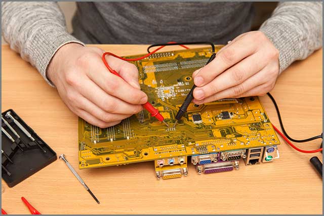 Image 2:A PC motherboard that carries large currents to the CPU
3. Design Tips for High Current PCBs
Here are some design tips for high current boards.
Removing solder mask
It is an inexpensive or rather free method to increase the current capability of a trace, and a path can have its solder mask removed, which then exposes the copper underneath. Then additional solder can be added onto the trail, which will increase its thickness and bulk and lower resistance.
It will then allow more current to be carried by that trace without increasing the trace width or paying extra for additional copper thickness.
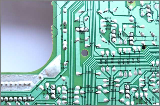 Image 3: PCB with a section of solder mask on a trace removed and additional solder added
Using polygon pours under high current components.
Individual components, such as large FPGAs and Processors, have extensive current requirements and many power pins. They also often come in BGA and LGA packages.
A trick to get enough current to them quickly is to have square polygon pours right under the chip and then having Vias drop down and connecting to them. You can then click the polygon pour to a thick power trace.
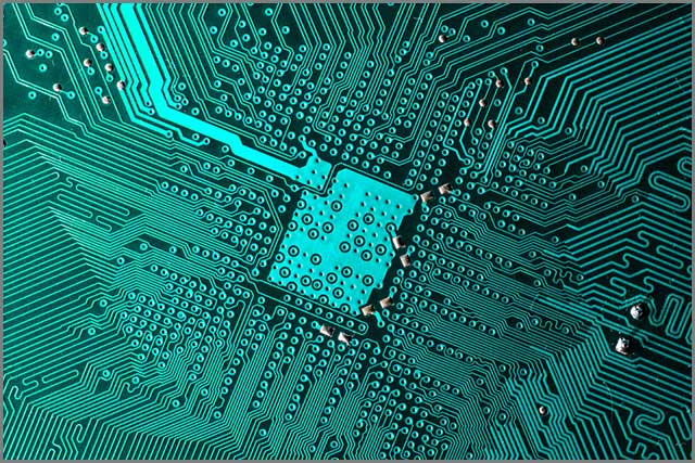 Image 4: Large Polygon Pour under a BGA chip for high current capability
Using internal layers for high current paths
If you run out of space for thick traces on the outer layers, it's often an excellent approach to have a solid fill in an internal layer and then use vias to connect to high current devices on outer layers.
Adding copper bars for very high current
In specific applications such as high power inverters and electric automobiles, the current can often be 100A or more. In such cases, it becomes pointless to use traces.
A common practice here is to use solderable copper bus bars that solder onto a PCB's pads and then carry most of the high current. Since the bars are much thicker than traces on a PCB, they can easily take an order of magnitude larger draft than regular hints while having around the same width.
Adding Via Stitching for Multiple Traces Carrying Large Currents
If a trace cannot carry the required current through a single layer, then the same path can be routed on an additional layer, and then via stitching can be done between the two layers. It effectively doubles the current carrying capacity assuming both traces on different layers have the same width.
A video explaining the process can see here:

4. What OurPCB Can Offer for High Current Boards
Rapid Prototype Service
High current boards often require multiple revisions before making a final large order.
OurPCB offers a rapid prototyping service, and you can order online by submitting your designs for a low cost and get your fabricated PCB in a short time.
We can produce quick turns to meet 72-hour delivery for 12-layer PCBs and 120 hours for 12+ layer boards.
Quick Online Quotation System
OurPCB offers an online quotation system, and you can request a free PCB quote. Our dedicated account managers will ensure you receive the support you need within minutes. We offer personalized, one-on-one services to help your project stay on schedule, whether it’s a custom or standard PCB quote.
Superior Materials
OurPCB offers a selection of PCB materials that are perfect for high-current, high-frequency, high-speed, and other special PCB substrate types designs.
| Brand | PCB materials |
|---|---|
| Rogers | PTFE-based: RO3000 series, RT series Non-PTFE: RO4000 series, Kappa 438 Thermoset Ceramic-Filled Resin: TMM series Prepreg types: RO4400 series, 2929, RO1200 |
| Panasonic | R5775 (M6), R5785 (M7), R5795U (M8) |
| Shengyi Technology (SYTECH) | S1600, S1165, S1151G, S1150G, SH260, ST210G, S0401N120, S7136, S7439, S7040GSynamic 6 / Prepreg Synamic 6B, LNB33, ST115 / ST110G, SJ series |
| Arlon | PTFE-based: AD series, AR series, Diclad series, TC series Hydrocarbon + Ceramic Filled: 25N / 25FR PI (Polyimide): 33N Prepreg types: 25FR / 25N, 91ML, 92ML |
| Taconic | PTFE-based: TLY series, TLX series, RF-35, RF-30, CER-10 Bonding films: HT1.5 (thermoplastic adhesive film), FR28 |
| Nelco | PTFE-based: NX9000, NH9000, NY9000, NH9000-13RF Non-PTFE: N4350-13, N4380-13 |
| Taizhou Wangling | PTFE-based: F4BK, F4BM, F4B-1/2, F4T-1/2 (pure PTFE) Special organic-polymer ceramics: WL-CT330 (338, 350, 440, 615) Composite dielectric materials: TF-1/2, TP-2 Bonding films: F4-PP250, WL-PP350 |
| Zhongying Technology | ZYF300CA-C, ZYF300CA-P, ZYF-CA |
| Fushide (FSD) | FSD-GX, FSD-NX, FSD-CX, FSD-TX, FSD615NT Bonding film: FSD28 |
| Isola | FR408HR, 370HR, etc. |
| TUC (Taiwan Union Technology Corporation) | TU933+, TU883, TU-872SLK, TU863+, TU-862, TU901, TU865, TU-768, TU-752 |
| EMC (Elite Material Co.) | EM526, EM528, EM888K, EM890/890K, EM891/891K |
| ITEQ | IT988GSE, IT968G, IT958G, IT170GRA2 |
| Ventec | VT-41, VT-42, VT-47, VT-481, VT-901, VT464/463 (high-speed), VT3703/VT870 (high-frequency) |
| Gospell | PTFE-based: GT-3000 series Bonding films: GT-3150DW, GT-1000 series |
| Relong | Commercial-grade: R200 series, RC300 series, RC400, RC600, RNF series Military-grade: RD series, RP series, RS300A/B, RS300B Bonding films: RLP30 / RLP30G |
| Guoneng | GNA220, GNA255, GNC3002, GNC3003 |
| Yinghua | H-870G, Y-201TS, Y-201TSR, Y-206BSM, Y-209HS |
| Mitsubishi Gas Chemical | HL832NXA, HL820WHI |
5. Conclusion
High current PCBs are all about a careful design process and using all features and space onboard efficiently.
These types of boards have become more common in recent times and will continue to be so.
For more information, you can contact us immediately, and we are happy to serve you.
Special Offer: Get $100 off your order!
Email [email protected] to get started!