Digital technology requires miniaturized, reliable, and efficient devices to fit into our everyday lives. Complex medical, aerospace, and communications machines also require such properties to enhance their performance. One way to achieve these properties is by using embedded PCB. These PCBs are practical solutions to the density and complexity of modern electronic devices, especially in the mobile industry. For more insights, check out our detailed exploration of embedded PCBs, and don't forget to request a PCB assembly quote to get started!
Contents
- What is an Embedded PCB?
- Why Embed Components in PCB?
- Miniaturization
- Mechanical Reliability
- Improved Electrical Performance
- Reduced Costs
- Drives Innovation
- Factors That Affect Embedded PCB Design
- PCB Size
- Thermal Management
- Placements
- Types Of Embedded Components
- Integrated Module Board
- Embedded Wafer-Level Package
- Embedded Chip Buildup
- Chip in Polymer
- How are Components Embedded in a Printed Circuit Board?
- Laser Drilling
- Milling and Routing
- Direct Fabrication into the Dielectric Material
- Active Devices
- Passive Devices
- The Assembly Process for Component Embedded PCB
- Solder Pad Mounting
- Thru-Hole Mounting
- Embedded PCB Applications
- Summary
What is an Embedded PCB?
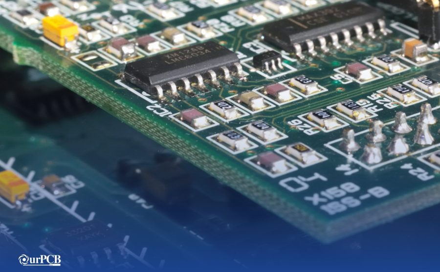
An embedded PCB is a circuit board containing embedded components for high performance and efficiency. Also, the embedding technology helps minimize transmission losses and reduces the interconnection paths between components to miniaturize PCBs.

An embedded PCB
Why Embed Components in PCB?
Embedding components on a PCB has the following benefits.
Miniaturization
Embedded components in flex and rigid reduce the number of parts to mount on the surface layers. Also, they can minimize the PCB size or enable you to fit more components on the same board size.
Mechanical Reliability
Embedding components instead of soldering them creates fewer solder joints that can fail. Thermal dissipation is also easier in embedded parts because you can place the components in direct contact with hole vias.
Improved Electrical Performance
Embedding allows you to place components in line to the signal path beneath the connecting paths. Therefore, you can reduce the connection path length between the two. Besides, this path reduction improves the signal integrity and minimizes the inductance & capacitance that create noise in a power signal network. Additionally, it reduces the parasitic effects in high-frequency circuits. EMI shielding is also easier on embedded components because you can surround them using the ground hole vias.
Reduced Costs
Embedded components require less assembly work than when dealing with thru-hole or surface mount technologies. Therefore, it can save on costs, especially for high-density PCBs requiring complex manual assembly.
Drives Innovation
Reductions in cost and size automatically push for innovations in PCB technology.
Factors That Affect Embedded PCB Design
The following factors affect the design of embedded circuit boards.
PCB Size
First, the PCB layout and size must match the active and passive components you will install on the board. Therefore, the PCB's dimensions should accommodate proper component placement and minimize the chances of overheating.
Thermal Management
A high current trace generates a lot of heat in a PCB. But you can improve thermal dissipation in the board by increasing the trace's thickness or building copper planes.
Placements
It is better to mount heavy components on the board's side to minimize mechanical tension on the soldering pads. Also, consider spreading out the power devices across the PCB's surface.
Special Offer: Get $100 off your order!
Email [email protected] to get started!
Types Of Embedded Components
Embedding chips in circuit boards can take any of the following approaches.
Integrated Module Board
First, IMB requires you to align the components. After that, lay them in a cavity and use controlled depth routing to place the hole in a core laminate. Next, fill the cavity using a molding polymer for electrical, chemical, and mechanical compatibility with the substrate.
Isotropic solder filling into the polymer helps create reliable solder joints when laminating the embedded component.
Embedded Wafer-Level Package
EWLP involves performing all technology steps and mounting components at the wafer level. The process limits the IO area to the chip's footprint size and requires a fan-in.
Embedded Chip Buildup
ECBU requires mounting chips on polyimide films, then building the interconnecting structures afterward.
Chip in Polymer
This process involves embedding thin chips into the dielectric layer during fabrication instead of integrating them into the internal layer. You can use standard laminated substrate materials in this process.
How are Components Embedded in a Printed Circuit Board?
You can embed passive and active components using one of the following processes.
- First, component molding into the substrate
- Second, placing components in internal cavities created in the PCB
There are several ways to create cavities in a circuit board. They include:
Laser Drilling
Laser drilling can create a cavity to a precise depth. After drilling, add a conductive adhesive material to hold the component in the hole. Lastly, melt the adhesive by heating to create a strong solder bond with the embedded part.
Milling and Routing
Milling and routing is another alternative for cavity creation. However, the equipment's shape and size will restrict the cavity size.
Direct Fabrication into the Dielectric Material
This process does not require routing or drilling. It is possible to fabricate some thin wafers directly into the PCB's dielectric layer.However, considering passive and active components, you can embed them in the following ways.
Active Devices
Semiconductors usually sit in a cavity. As a designer, you must line up the die bonds carefully. The goal is to create a short & direct connection between this component and the external one. There are two ways of embedding the IC. First, you can fill the cavity with a polymer material to fix the chip into the substrate. Secondly, you can preinstall it into the dielectric material during fabrication.
Passive Devices
It is possible to embed passive components into PCBs using different copper foil, conductive ink, and dielectric material values. Design these parts into the board during the design process and specify the materials for each component.
The Assembly Process for Component Embedded PCB
The assembly process for mounting components in embedded PCB involves solder pad and thru-hole mounting methods.
Solder Pad Mounting
This process involves bare dire and chip mounting. The first method involves flip flop or wire mounting processes. However, you can use conductive resin or wave soldering with chip mounting.
Thru-Hole Mounting
Thru-hole mounting also entails bare dire and chip mounting methods. However, these processes have either conductive adhesive or plated thru-hole options.
Embedded PCB Applications
- Computer processors
- Wired and wireless broadband systems
- Healthcare machines (X-ray, ultrasound, fitness devices, magnetic resonance imaging, etc.)
- Backplane technology
Summary
In conclusion, embedded PCBs require a little more work to mount the components into the inner layers. But the benefits are worth it. We hope you have learned a lot from this article. If you think we have left something out, leave a comment in the chat/message section, and we'll get back to you asap.
Back to top: Embedded PCB
Special Offer: Get $100 off your order!
Email [email protected] to get started!