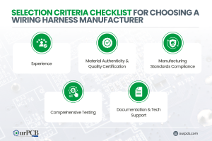
Top 10 Classic Car Wiring Harness Manufacturers | Full Guide
Finding the right wiring harness manufacturer for your vintage ride can be a real headache. Those beautiful old machines need special wiring that looks period-correct

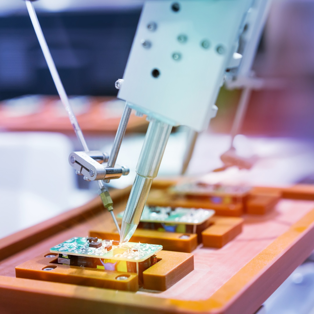
OurPCB specializes in custom PCB assembly, delivering tailored solutions for unique designs and specifications. We offer precision SMT, through-hole, and mixed technology assembly with prototyping and full-scale production. Expect rigorous testing, fast turnaround, and scalable PCB manufacturing to meet your exact requirements. Want to dive deeper? Explore PCB Components and how they influence your PCB assembly design.


OurPCB specializes in fully customized PCB assembly for medical devices, automotive systems, aerospace technology, and industrial equipment. We tailor every board to your exact specifications, ensuring precision, reliability, and fast turnaround from prototyping to full production.
| Specification | PCBA Capability |
|---|---|
| Placer speed | 600,000 chips/hour |
| Lead Time | 25+ Days (To Be confirmed) |
| SMT | SMT, Through Hole Assembly Single/Double-Side SMT, Single/Double-Sides Mixture Assembly |
| PCB Size | 50mm×50mm ~610mm×508mm |
| PCB Thickness | 0.5mm~4.5mm |
| Min. diameter /space of BGA | 0.2mm/0.35mm |
| Qualifications | ISO 9001:2015 |
| Accuracy | <±30µm, under the condition of 3σ,CPK≥1 |
| Minimum width/space of QFP | 0.15mm/0.25mm |
| Minimum Diameter /Space of BGA | 0.2mm/0.35mm |
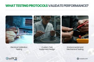
| Reliability Test | Flying Probe Test/Fixture test, Impedance Test, Solderability Test, Thermal Shock Test, Hole Resistance Test, and Micor Metallographic Section Analysis, etc. |


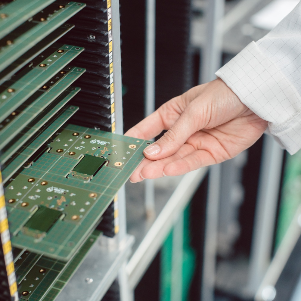
At OurPCB, we understand that one size does not fit all. Our commitment to customization allows us to work closely with our clients to develop PCBs that align perfectly with their product specifications. Here are some key aspects of our customization capabilities:

We offer a wide range of materials suitable for various applications. OurPCB utilizes high-quality substrates such as FR-4, polyimide, and other specialized materials that can withstand high temperatures and provide excellent electrical insulation. This flexibility ensures that your custom PCB can perform optimally in its intended environment
Depending on your product’s complexity, we can design single-sided, double-sided, or multilayer PCBs. Our expertise in layer stack-up optimization helps achieve the desired electrical performance while minimizing costs
We provide various soldermask colors and silkscreen printing options to enhance the aesthetic appeal of your PCBs while ensuring functionality. This customization not only helps in brand recognition but also aids in the identification of components during assembly
In cases where the schematic may not be available, the data created from the printed circuit board reverse engineering can be used to produce replacement parts or give hints in repairing parts that already exist.
OurPCB caters to a diverse range of industries, each with its unique requirements for custom circuit boards:
If you’re curious about PCB Assembly vs PCB, we can guide you in making the right choice based on your industry’s requirements.

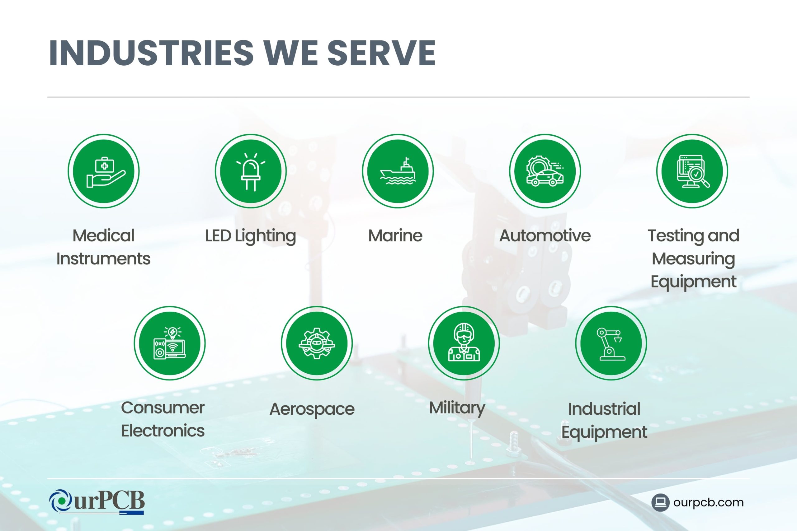
OurPCB caters to a diverse range of industries, each with its unique requirements for custom circuit boards:
If you’re curious about PCB Assembly vs PCB, we can guide you in making the right choice based on your industry’s requirements.
At OurPCB, we believe in fostering innovation through collaboration. If you have a unique idea for a product but lack the design expertise, our team of skilled engineers is here to help. We offer comprehensive design support, including:
At OurPCB, we believe in fostering innovation through collaboration. If you have a unique idea for a product but lack the design expertise, our team of skilled engineers is here to help. We offer comprehensive design support, including:
We handle everything from parts sourcing to final assembly, providing a hassle-free experience that ensures top-quality boards every time.
Whether you need a few prototypes or large-volume batches, our flexible assembly services adapt to your project’s scope and timeline.
Stay environmentally responsible with our compliant assembly processes, offering RoHS and lead-free options for safe, reliable builds.
No matter the complexity, we can assemble boards of all configurations—single-layer, multi-layer, or a mix—to match your exact specifications.
From one-off prototypes to bulk orders, we accommodate projects of all sizes without compromising on quality or turnaround time.
Join our growing community of satisfied clients who rely on our dependable assembly expertise and dedicated customer support.
Mon-Fri: 24 hours,
Sat: 9am-6pm, GMT+8
Reach us at
[email protected]
24 hours online
+86-199-30589219
Mon-Fri: 24 hours,
Sat: 9am-6pm, GMT+8
PCBs are composed of multiple layers bonded together, including:
Different materials, such as fiberglass, epoxy, or phenolics, are used based on application needs, ensuring durability and performance.
Finding the right wiring harness manufacturer for your vintage ride can be a real headache. Those beautiful old machines need special wiring that looks period-correct
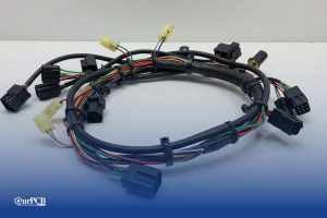
Would your car be able to run without wire harnesses? Not a chance. Wire harnesses connect all the electrical parts together. No harness means no
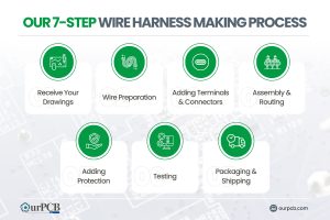
Making wire harnesses isn’t complicated. At OurPCB, we create custom wire harnesses for an expansive range of industries every day. While it’s a complicated process,
Prototype cable assemblies are the very important place in between PCB design ideas and interconnects. OurPCB brings prototype assemblies with PCB solutions to your tables.
PCB thermal management prevents component overheating through strategic heat transfer techniques. Without proper thermal control, electronics are at risk of electronic failures through weakened solder
ContentsKey TakeawaysWhat is a Multilayer-Printed Circuit Board?How do Multilayer PCB Boards Work?Multilayer PCB ApplicationsMultilayer PCB Manufacturing Process: StepsMultilayer PCB Manufacturing MachinesBenefits of Multilayer Circuit BoardsWhat
We use cookies to improve your browsing experience, which may include personal information. By clicking "Agree," you accept our Privacy Policy and cookie use. You can change your cookie settings in your browser anytime.
Agree
 Chat With Us
 Free Quote