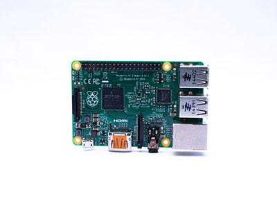
In microelectronics, custom printed circuit board designs come in different forms and shapes. Often, it depends on the purpose of the printed circuit board and the electronic components used in assembly processes. But two parts of the same PCB panel sometimes have different functions. Therefore, when detachment is needed at a later point, perforated breakaway tabs PCB is the ideal solution. To enable this breakaway feature, manufacturers put holes at specific dimensions. Ultimately, the purpose is to increase flexibility in PCB assembly and dismantling. Further on, you learn all about breakaway tabs PCB and how to get the best of it.
Contents
What is Breakaway Tabs PCB?
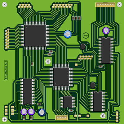
Breakaway Tabs PCBs are array boards with a little row of holes perforated into them. They are two types: the Mouse bites and the V-groove method.You produce mouse bites when you use break-routing or break-off tabs. The resulting perforated boards then allow smaller boards for use as an array. After depanelization, the board outline has rough edges that look like postage stamp holes; hence, the name Mouse Bites. A typical application, in this case, is in FR4 panels. Unlike the mouse bites, however, a V-Groove PCB has smooth edges. It is a suitable alternative for most designers looking for a smooth board edge with a tab-routed panel.
Special Offer: Get $100 off your order!
Email [email protected] to get started!
Breakaway Tabs PCB's best approach
There are three primary ways to achieve a PCBA breakaway tab.
They include milling depalletizer, V-groove depalletizer, and the physical method.
Milling depalletizer
In most cases, the milling depanelized, or tab routing has the best method.
It overcomes the difficulty around directly isolating the V-groove.
Usually, this method uses a milling machine at high velocity for the cutting process.
The milling machine guarantees increased quality and decreased scraps overall.
However, the disadvantage of the milling depalletizer is the cost and the programming required for the work.
(A high-precision milling machine for perforating rat-bite rows).
V-groove depalletizer
Unlike the milling depanelizer, this method is less expensive.
It involves cutting along the PCBA V-groove with a blade tool.
However, making a straight cut along the row requires maximum carefulness. The V-cut blade remains relatively costly still.
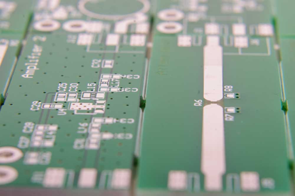
(A V-groove circuit board).
The physical/manual method
The last method is to break away the PCB tab by hand.
Otherwise, a needle-nosed plier or other segmentation tools would be handy.
Although this method is the least expensive and the easiest, it is risky.
Often, the PCB breakaway tab breaks into bits in the process.
The physical method is best if you work with small quantities of low-cost PCB boards.
For bigger PCB depanelizing, advanced tools are necessary.
How to indicate PCB designs with Breakaway Tabs
One of the best ways to achieve this is to design V-grooves that go more than halfway through the PCB.
Creating perforation holes in a PCB (mouse bites) is not difficult.
However, the routing process involved in producing a breakaway tab with the right balance is time-consuming.
Also, the PCB must not be too tough to break, nor must it be too weak.
Otherwise, it damages easily and produces an irregular shape.
Therefore, to get the right perforated breakaway tabs, use these dimensions:
- For unplated holes, use a drill diameter of 0.015".
- Introduce a 0.025" spacing from the drill center of one spot to the other.
- A max distance of 0.118" spacing between breakaway tabs further helps use of depanelizing tools.
Do you prefer a stronger tab? Then, consider adding extra spacing between the holes. If you get it right, the boards break regardless of PCB thickness or torque.
Other Considerations
In general, PCB breakaway tabs require care when designing them.
The aim of the design is such that it is possible to assemble other PCBs into one and later break them apart.
So to get the right breakaway tab design, here are a few steps you should consider.
Obtain the footprint.
This step involves sourcing the PCB breakaway design needed with dedicated software.
Place the footprint.
Next, you need to simulate the obtained footprint.
That is, you determine the board outline by marking out the edges to be cut.
Mark guidelines to match the breakpoints.
This final step involves making small indents so that the tab breaks when you apply the proper force regardless of material thickness.
Conclusion
The idea behind breakaway tabs PCB is to enable quick and automated board assembly.
Not only can we use them to assemble several small PCBs, but we can use them to add tooling holes, rails, and fiducials.
In most cases, the application determines how you produce the array boards.
However, designing the optimum breakaway PCB panel requires attention to minor details.
Are you looking for assistance with your PCB assembly?
We are helping to help! Contact us today.
Special Offer: Get $100 off your order!
Email [email protected] to get started!