Different designs and techniques come into play for PCB production. Some boards are flat, while others have little notches like the mouse bite PCB. But the big question is: which of these PCBs are ideal for your projects?
This article will talk extensively about the major designs and help you make a more informed decision. Also, you’ll learn about other things like PCB panelization, the difference between the different fabrications, and more.
Let’s begin!
Contents
- What Is Mouse Bite in PCB?
- Mouse Bite PCB: Location, Dimension, Sizes
- Things to Consider During Placement of PCB breakaway Tab
- PCB Panelizations
- Factors to Consider Before Performing PCBs Panelization
- Materials
- Design
- Tips on Preparing for PCBs Panelization
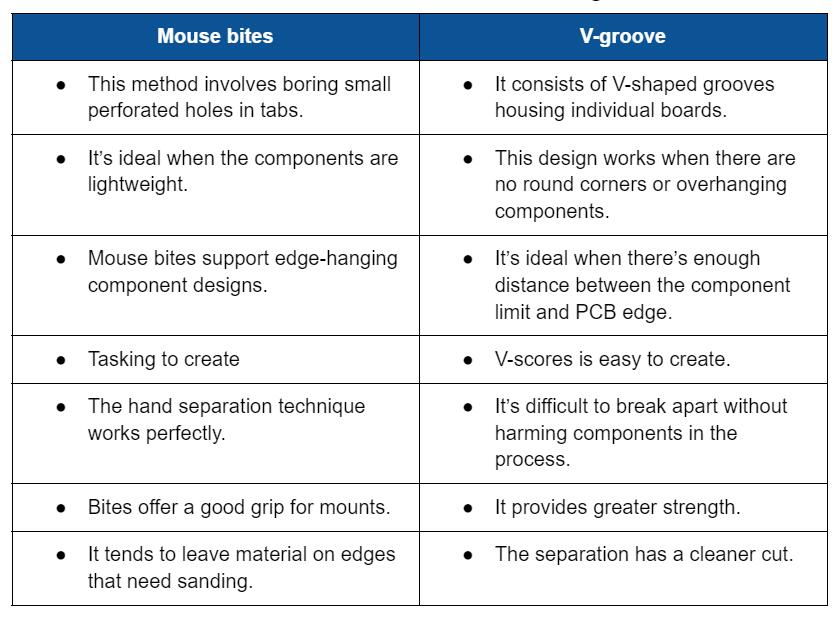
- The Difference Between Mouse Bites and V-groove PCBs
- Breakaway Tab PCB: Panelization Methods
- Types of PCBs Panelization
- Tab Routing Vs. V Groove PCB Panels
- Mouse Bites PCB: Board Shapes
- Mouse Bites PCB: Waste
- Mouse Bites PCB: Edge Quality
- Mouse Bites PCB: Timing
- Final Words
What Is Mouse Bite in PCB?
Mouse bites in PCBs refer to little perforations on boards. In addition, mouse bites look like half holes on a postage stamp. So, these perforations allow small boards to connect in a group. You can also call the holes perforated PCB breakaway tabs.
These holes help to improve the grasp of a board during mounting. A remarkable benefit of these holes is that they allow manufacturers to process numerous boards in the panels for one price. When the production process is over, fabricators separate the boards via depanelization.
Also, depanelizing is a walk in the park thanks to the tabs that break along the hole on the board. So, whatever remains of the board will look like a mouse bite.
Mouse Bite PCB: Location, Dimension, Sizes
Most times, the holes on breakout tabs vary. But most boards have five holes in the breakout tabs. Typically, the hole size in diameter is about 0.020 inches or 0.5mm. As for spacing, the holes are 0.030 inches or 0.76mm apart. But some boards don’t follow these specifications.
So, you may come across random sizes and spacing of the holes. Surprisingly, there’s a good and bad side to random sizes. For instance, if the mouse bites are tiny, it’s less stressful to smoothen out. But it also means that you may need more holes.
And if the holes are too large, it will take more effort to smoothen the bites. Overall, the goal is to have a board with an accurate hole placement, adequate size, and dimension. That way, there will be less material leftover to remove.
Things to Consider During Placement of PCB breakaway Tab
Before you use the perforated breakout tabs around a board’s outline, it’s important to follow the rules below:
- It’s ideal for saving effort and time on the router bits by avoiding using many tabs.
- Throughout a PCB assembly, it’s vital to ensure that the panel has sufficient tabs that can sustain the PCB completely.
- If you have tabs with a minimum clearance of about 0.1125 inches, ensure that it’s near the closest components.
- Ensure that the tabs are far from sensitive component areas or circuitry to avoid breakout stresses.
With that in mind, it’s crucial to note that if stress scarring affects the circuitry due to the tabs breaking, you may not notice it early. And it may cause recurrent issues that are hard to debug.
Further, if you don’t use adequate tabs or position them tactically during the production process, the board will flex excessively. As a result, you may have an unstable assembly.
Special Offer: Get $100 off your order!
Email [email protected] to get started!
PCB Panelizations
The PCB penalization
PCB penalizations are the opposite of depanelization, and it refers to connecting smaller circuit boards into a large group. With this process, your aim should be to arrange a maximum number of boards to fit tool restrictions.
You can prepare your board for panelization by placing fiducial markers on the opposite corners of the panel and board.
The markers are effective for pattern recognition. And they also help to verify your board’s orientation, reject boards below standard, and measure distances on the board.
Factors to Consider Before Performing PCBs Panelization
Materials
Before using a panelization method, consider your PCB material. For instance, a CNC router is ideal for dealing with extremely thin and wide boards that can’t handle excess mechanical stress.
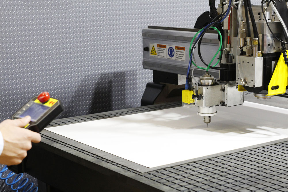
CNC router
Design
Confirm the type of design you’re working with before choosing a panelization. So, if you’re working with a board with edge-hanging components, it can affect your panelization choice.
Tips on Preparing for PCBs Panelization
- To avoid a deformity after placing the panel on a fixture, ensure that the external border of PCB penalizations has a closed-loop design.
- The PCB penalizations close to a square is ideal, e.g., 3 x 3.
- Control your center distance between the panels, positioning them to lie within 75mm to 145mm.
- Your PCB panelization should be ≤ 125mm × 180mm for automatic dispensing.
- Ensure that the non-resistive soldering area exceeds your mark point.
- The connection bridges between the pieces should be void of protruding or large devices. Also, your components and borders shouldn’t have over 0.5mm to avoid damage.
- Place your huge components in positioning post holes like headphone interface, I/O interface, etc.
The Difference Between Mouse Bites and V-groove PCBs
Breakaway Tab PCB: Panelization Methods
The breakaway tab PCB, like the name suggests, isn’t part of the PCB. So, you can add it to two or four sides of the board to help in SMT assembly. After the assembly, the tabs go off.
Types of PCBs Panelization
V-cut (V-grooves)
V-grooves
The V-grooves are the most common type of PCB penalizations that has a depth of about 1/3 of PCB thickness on two sides of a PCB. Also, it has a router bit of 30 or 45 degrees. Additionally, this PCB penalizations help PCB panels gain mechanical strength during production. And it’s quite easy to separate the panels after assembly.
This PCB panelization is ideal for PCBs with two parallel edges like the rectangular board. After the whole process of depanelization, the unit board’s edges have good uniformity. In addition, the distance between adjacent V-cuts shouldn’t be less than 1mm. And the minimum thickness of the PCB center should be greater than 0.4mm.
Also, your misalignment of the upper and lower V-cuts shouldn’t be less than 1mm. So, if you’re working with a board with a thickness of less than 1.2mm, the V-cut isn’t ideal.
Routing Tabs (Stamp Holes)
This method is the perfect go-to if you’re working with irregular edges. Further, it involves using a bridge that’s wide on both ends. While at it, you have to use a bridge with a narrow middle.
Also, the bridge should be wide on two ends. And the breakaway tabs should feature a row of mouse bites at the edge of the bridge. Interestingly, this PCBs panelization method may result in edge burrs and need special attention during the designing process.
The things needed for the routing tabs are as follows:
1. Your routing tab should be between the unit and the breakaway tab without traces.
2. The traces on both sides of the via should be in different layers. Also, it’s vital to keep your trace width above 0.3mm.
3. Ensure that the routing tab is between units that lack V-cuts.
It’s crucial to know that these methods need a distance of two tabs between 6 to 40mm.
Solid Tab Panelization
With this method of panelization, you can design groups or arrays with solid tabs between the boards that enhance the overall strength. But this method requires a depaneling router, laser cutting machine, or blade tool.
Further, this bladed tool is the most cost-effective option, but it has issues with blade rotation, which is inefficient. In contrast, laser-cutting is more expensive. But it doesn’t work on PCBs that are over 1mm thick.
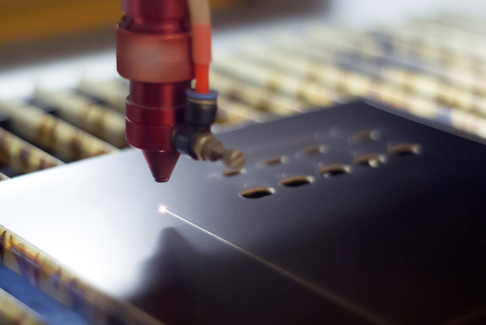
Laser-cutting machine
Tab Routing Vs. V Groove PCB Panels
Before you choose any of these methods, consider your PCB design and the following factors:
Mouse Bites PCB: Board Shapes
V-cut PCB panels are perfect for working with square or rectangular boards. But tab routing is better if you’re working with irregular shapes.
Mouse Bites PCB: Waste
V-grooving is a better alternative because it wastes fewer materials than tab routing.
Mouse Bites PCB: Edge Quality
If this is a criterion for your work, tab routing is better than V grooving. But you may have small rough laminate rubs that require sanding with this process. On the other hand, V-cuts have rough edges that require more sanding to get smooth edges.
Mouse Bites PCB: Timing
V-groove is the ideal option to finish up in less time. And it takes more time to set up the tab routing.
Final Words
Mouse bite PCB is a great addition if you want boards with grip when mounting. On the other hand, V-groove is an excellent choice if your project requires greater strength.
So, do you need help getting the best panels that meet your specifications? Please feel free to reach ourPCB.
Special Offer: Get $100 off your order!
Email [email protected] to get started!