We will look at selective gold plating and its importance in PCB fabrication & assembly in this article.
Gold plating is vital in electronics because the metal has two unique properties not found in other metals.
- High resistance to corrosion
- Low contact resistance
So circuits coated in this material last longer and withstand extremely harsh operating conditions without breaking down.
However, the material is expensive. So PCB manufacturers try to use as little gold as possible to keep the costs down.
Therefore, they do selective gold plating, and we’ll look at what the process entails below. Let’s get right into it!
Contents
- What Is Selective Gold Plating?
- Selective Gold Plating Methods
- Finger-Plated Electroplating
- Reel-Selective Plating
- Through-Hole Electroplating
- Brush Plating
- Why Place the Selective Gold Plating Above a Nickel Layer?
- Pros and Cons of Selective Gold Plating
- Pros
- Cons
- Are Selective Gold Plating and Immersion Gold (ENIG) the Same?
- What About Soft Gold Plating?
- Selective Gold Plating Applications
- Wrap Up
What Is Selective Gold Plating?
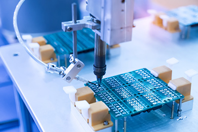
Manufacturers rarely use a full-body hard gold finish on circuit boards because it is costly and has relatively poor solderability.
So the material gets applied on high-wear areas, such as the gold fingers on edge connectors. But it usually does not get applied to solderable areas.
Therefore, manufacturers place the gold surface finish selectively on the circuit.
This plating process is similar to the hard-gold surface finish process.
Gold mixed with hardeners gets applied over a nickel coat barrier via electroplating using an electric current.
However, the process requires more work due to masking to ensure only the required areas get the coat.
This process makes the labor costs higher than full-body hard gold surface finishing.
And in some instances, you might need to protect soldering pads using hard gold.
So when soldering, use a super active flux to clean the surface and give the best wetting.
Selective Gold Plating Methods
Manufacturers usually use either of these four methods for selective gold plating.
Finger-Plated Electroplating
Also known as protruding partial plating, the finger-plating process occurs using the following steps.
- Washing and rinsing using water
- Abrasive scrubbing
- Activation in 10% sulfuric acid
- Nickel plating on the finger contacts (4-5μm)
- Mineral water cleaning
- Treatment using a gold permeation solution
- Gold electroplating
- Cleaning
- Drying
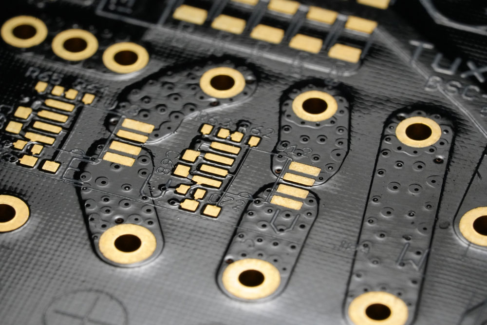
Gold-coated parts on a circuit board
If the finger connectors had a tin or tin-lead coat, strip this layer first.
Reel-Selective Plating
This plating method can be manual or automatic, But regardless, you must first coat the section of the copper that does not require plating with a resist film. After that, plate the exposed copper section.
Through-Hole Electroplating
Selective electroplating does not occur on fingers only. You can partially coat a via’s inner walls using a low-viscosity ink, which applies a highly conductive film.
Next, thermal curing forms a continuous film on these walls, after which you can electroplate the gold without additional processing.

A PCB with gold-coated vias/through holes
This process does not require multiple chemical treatments. Instead, you only need to do one ink application step.
Also, the resin-based ink has strong adhesion, making it easy to bond to thermally polished holes. So it eliminates the etch-back process.
Brush Plating
This electrodeposition technique does not immerse all the copper parts in the electrolyte. So only the area that requires coating dips into the solution.
Usually, a chemically reactive anode like graphite wraps around an absorbent material like cotton.
This setup brings the plated solution to the required electroplating area.
The method is typical in electronics PCB assembly shops to help repair waste boards.
Why Place the Selective Gold Plating Above a Nickel Layer?
Regardless of the selective gold-plating process, an underlying metal layer is necessary for mechanical backing. The most typically used metal is nickel.
Why use this barrier metal layer?
The base material used to create PCB traces and contact pads is copper. If you plate gold directly on copper, copper will diffuse into the gold.
So eventually, the gold layer will migrate, shifting below the copper. On the other hand, copper will rise to the top.
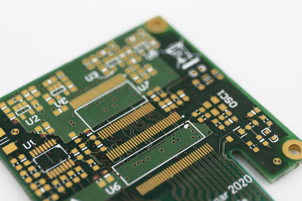
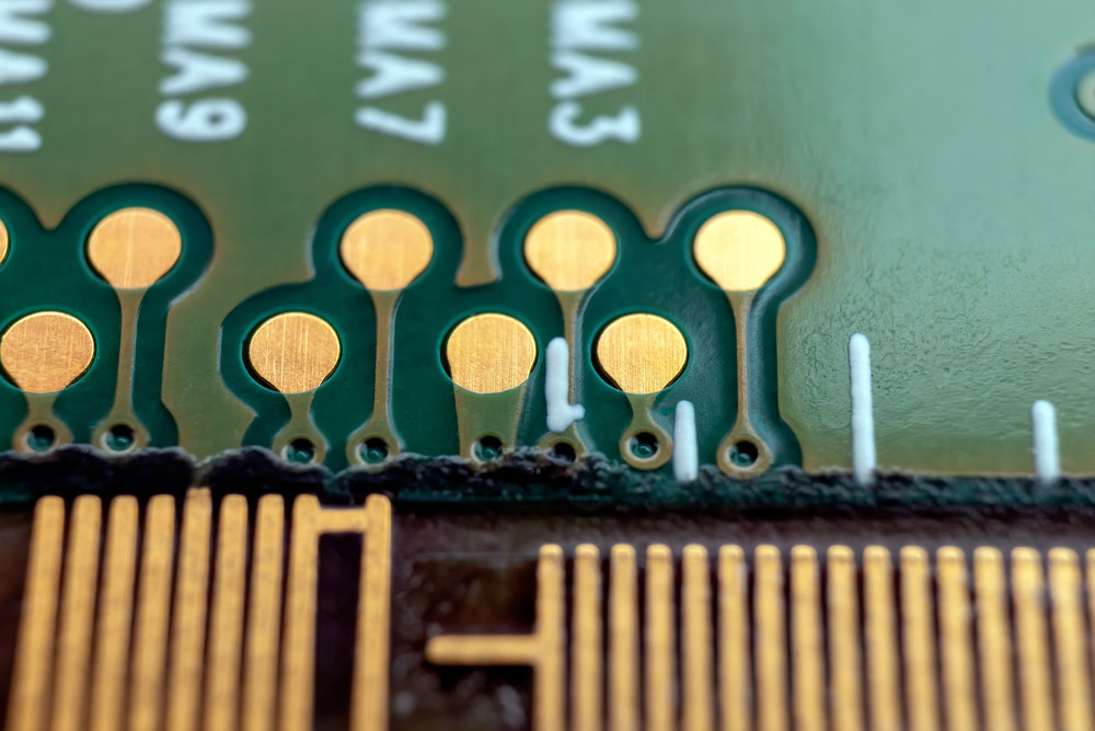
A circuit board with gold-plated pads and contact points
This shift will introduce one problem; the contact pad’s electrical conductivity will reduce significantly.
The exposed copper will corrode and oxidize, covering the surface with a non-conductive material.
So nickel creates a mechanical backing for the gold layer for better wear resistance.
Additionally, it minimizes the oxidation that can reach the copper layer if the gold has pores.
You can layer this nickel using either the electrolytic or electroless plating processes.
Special Offer: Get $100 off your order!
Email [email protected] to get started!
Pros and Cons of Selective Gold Plating
This gold-plating process has the following upsides and downsides.
Pros
- Creates a hard and durable surface
- Long shelf life (zero oxidation)
- Zero leads
Cons
- Expensive metal
- Complex process (labor intensive due to masking)
- Requires plating busbars
- Etching undercut can lead to flaking or silvering
- The gold surface finish does not cover the sidewalls (except in gold fingers)
- Unsolderable above 17 μin
Are Selective Gold Plating and Immersion Gold (ENIG) the Same?
The keywords here are plating and immersion. With selective gold plating, the process occurs through electrochemical plating.
This coating creates a hard gold surface, but gold takes up about 1% of the contents in the electroplated layer.
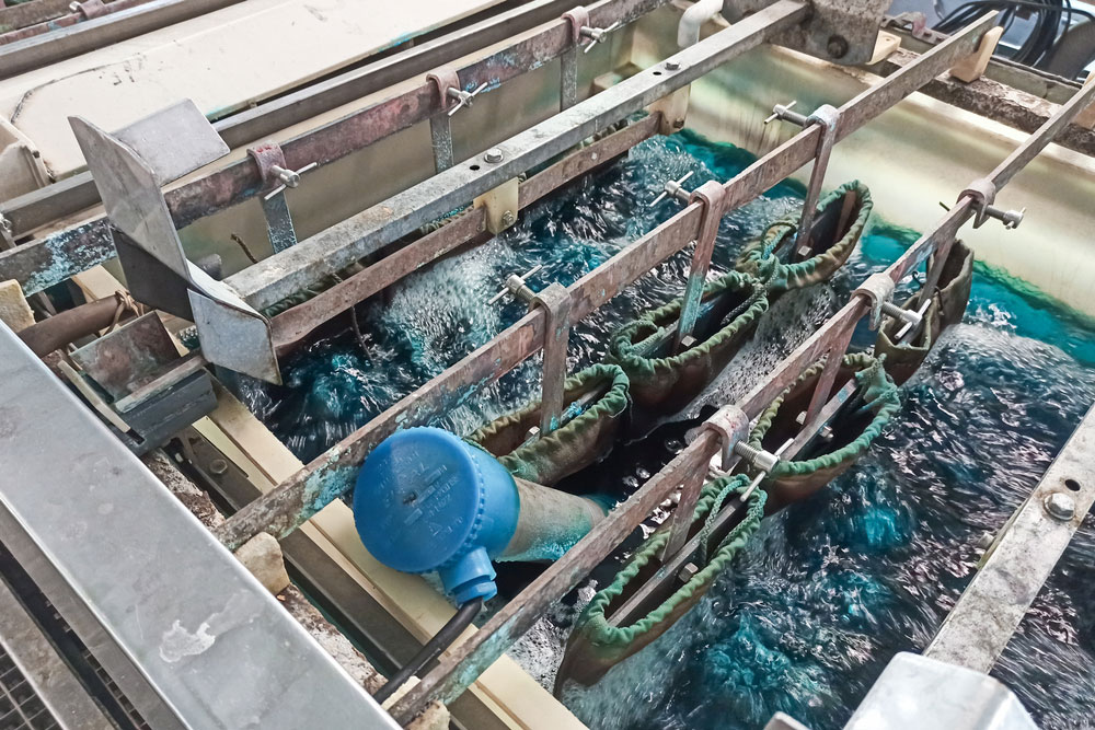
A copper electroplating machine for circuit boards
Gold is naturally a soft material, so the rest are hardeners, which make the layer hard and wear-resistant.
And the gold layer thickness is smaller than the one created by the immersion process.
On the other hand, ENIG involves depositing a nickel layer followed by a gold layer on pads using electroless chemical reactions. This process creates a thicker gold layer than the one formed by selective gold plating.
And the layer appears brighter because the gold used is pure but has no hardeners to make the surface hard and wear-resistant.
Also, the gold layer created in this process has better solderability than the one formed by selective gold plating.
Gold-coated contact pads on an LCD TV’s printed circuit board
What About Soft Gold Plating?
It is possible to electroplate pure gold, but it will create a thin layer that is not as durable.
So the surface will experience quick wear from contact switching, exposing the copper below.
Hard gold gets formed by adding non-noble metallic elements like nickel, cobalt, or iron.
These metals alter the electroplated deposit’s grain structure to be finer and more wear resistant.
The grains measure about 20-30 nm, while soft gold-plated grains are roughly 1-2 um (1000-2000 nm).
When comparing the hardness levels, the hard/selective gold plating can achieve 130-200 HK25.
But soft gold, including the immersion type, only goes up to 90HK25.
Selective Gold Plating Applications
Selective gold plating brings about four properties.
- Wear resistance
- Oxidation resistance
- Good conductivity
- Corrosion resistance
If your PCB requires these qualities, then go for selective gold plating.
For instance, keyboard and button circuit boards need these surface finishes to withstand multiple key presses repeatedly.
Selective plating is also ideal for making gold fingers (electrical connectors) on data storage circuit boards. Think of SSD and RAM cards.
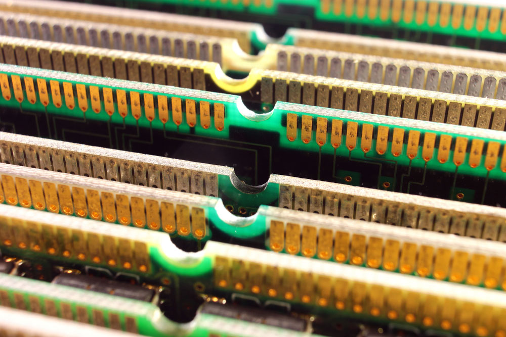
Gold fingers on SIMM and DIMM computer memory modules
Wrap Up
In conclusion, selective gold plating is the partial coating of hard gold on PCB pads.
Remember, the material is expensive, and the process is labor intensive.
So look for a reliable selective gold plating PCB manufacturer to get the job done.
At OurPCB, we have the required equipment and expertise to produce high-quality partial gold-plated boards.
Contact us today with your PCB designs, and we’ll be in touch to discuss the specifics.
Special Offer: Get $100 off your order!
Email [email protected] to get started!