What is diode breakdown voltage? Breakdown voltage is a critical property in electronic components like diodes. This property comes about when reverse-biasing the voltage across the diode’s terminals and gives the upper limit for the device’s application in electrical circuits.Let’s analyze the diode breakdown voltage to better understand this electrical property.
Contents
- What Is Breakdown Voltage?
- Diode Breakdown Voltage
- Forward Bias
- Reverse Bias
- Is Exceeding a Diode’s Breakdown Voltage Destructive?
- Factors Affecting a Diode’s Breakdown Voltage
- Physical Mechanism
- Doping Concentration/Profile
- Structure and Geometry
- Zener Diode Breakdown Voltage
- What About the Avalanche Breakdown?
- Wrap Up
What Is Breakdown Voltage?
This term can have slightly different meanings depending on the material. In insulators, for instance, it refers to the minimum voltage you can apply to the material to become electrically conductive due to experiencing electrical breakdown.But in diodes, the term refers to the minimum reverse voltage you can apply to the device to conduct electric current in reverse bias.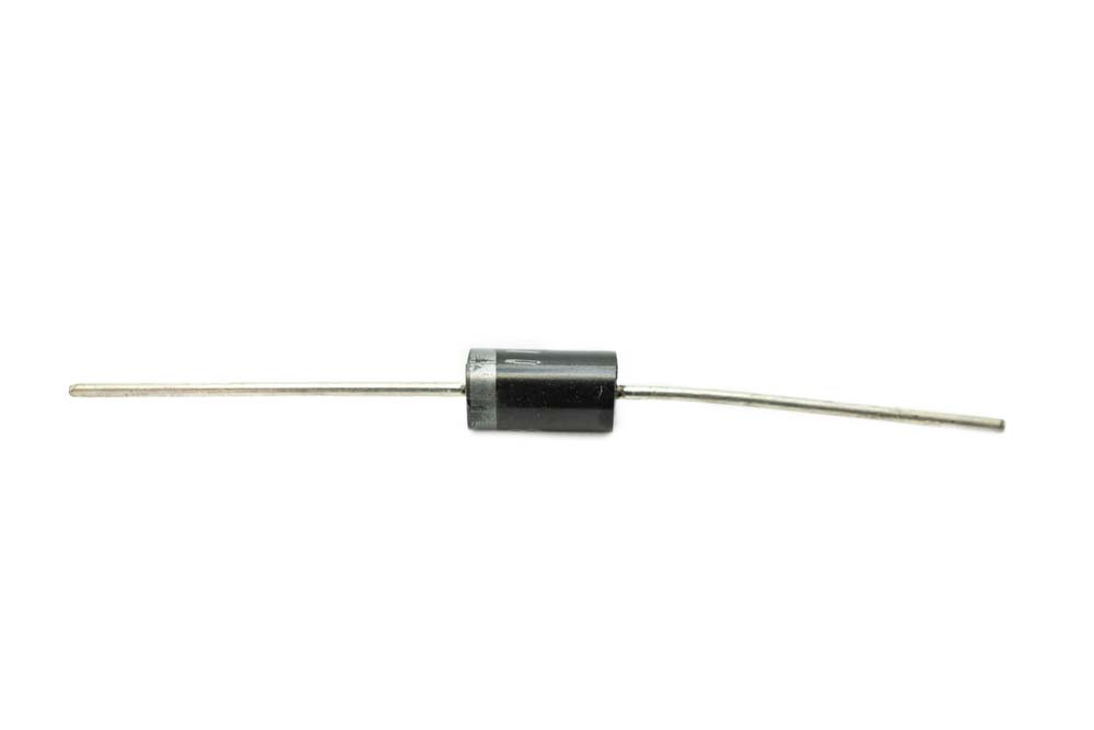
A diode
Breakdown voltage is a characteristic of insulators but can also apply to semiconductors because their electrical properties lie between conductors and insulators.Therefore, the breakdown voltage level differs depending on the material’s physical properties. It is also known as the material’s dielectric strength.
Diode Breakdown Voltage
Diodes fall in the semiconductor category and have a PN junction consisting of P-type and N-type sides. The P-type semiconductor side contains group IV elements like silicon doped with Indium or Boron. This doping leaves them with an electron-hole charge carrier.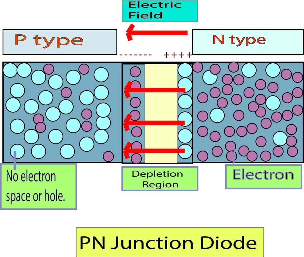
A PN junction highlighting the majority and minority charge carriers on either side and the depletion layer in between
N-type semiconductors contain the same group IV element but have Phosphorus, Antimony, or Arsenic doping. This doping leaves the material with an electron charge carrier.The two have a bandgap (depletion layer) at the junction where the exchange of charge carriers occurs.
Forward Bias
In forward bias, the positive voltage gets applied to the P-type terminal, and the N-type connects to the power source’s negative terminal. This connection places the applied voltage opposite the junction barrier’s potential, making the majority of charge carriers flow across the junction.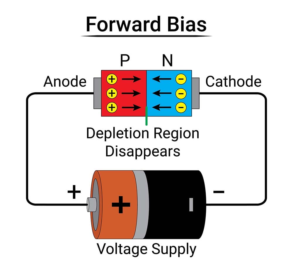
A diode connected in forward bias
The voltage required to make these charge carriers flow across the junction is low because the depletion layer width decreases/disappears.
Reverse Bias
The diode should not conduct electricity if you connect the terminals in reverse (positive voltage to N-type and negative voltage to P-type).However, that is not the case. Since the doped semiconductors have a small quantity of minority charge carriers, some electric current (leakage current) will flow.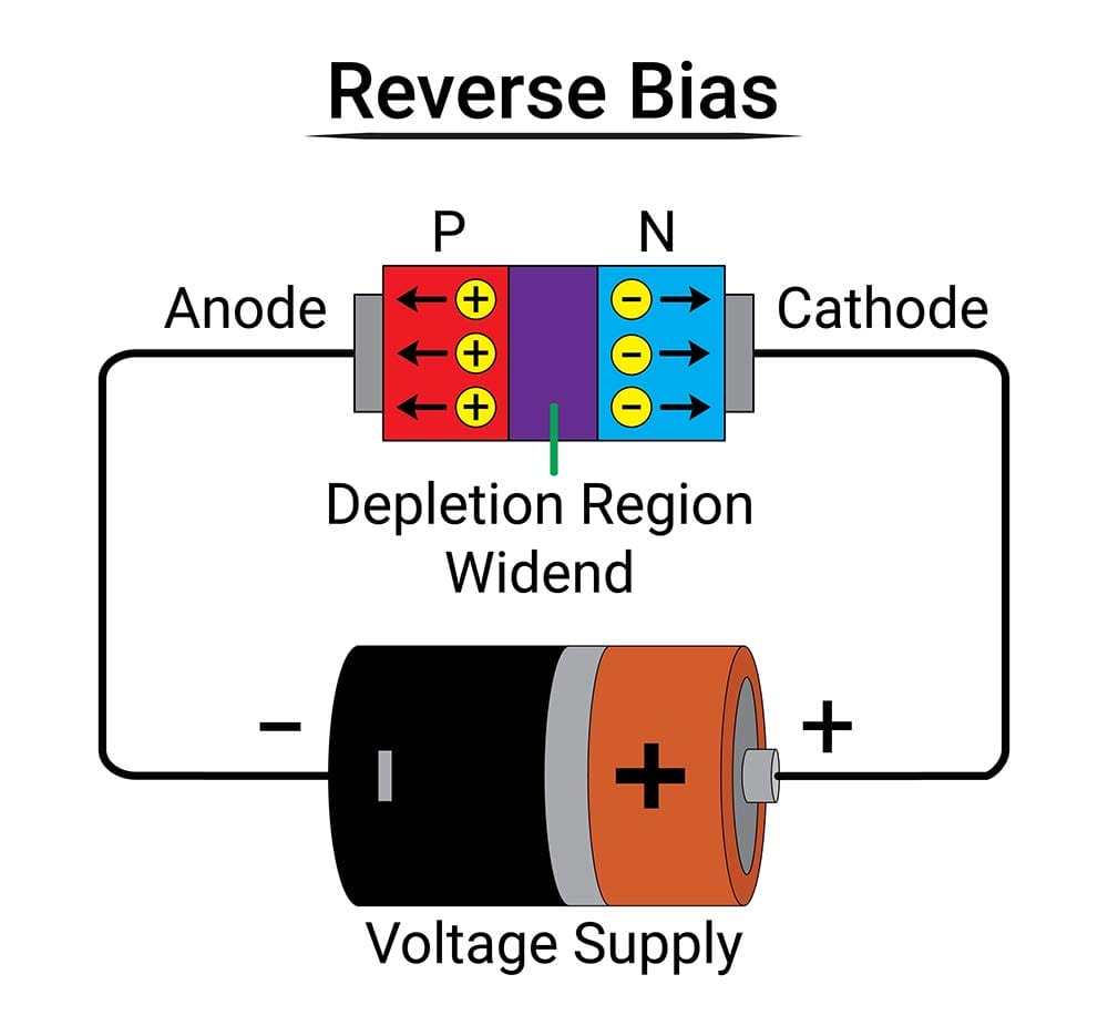
A diode connected in reverse bias
This reverse current increases the width of the depletion layer barrier. As you increase the reverse bias voltage, it will reach a point where the reverse/leakage current rapidly increases.This condition is known as junction breakdown; the minimum voltage that gets you to this point is the diode’s breakdown voltage. Some refer to it as the reverse breakdown voltage.Therefore, you can define a diode’s breakdown voltage as the highest reverse voltage you can apply across a diode’s terminals without causing an exponential increase in the leakage currents.
Is Exceeding a Diode’s Breakdown Voltage Destructive?
Exceeding the diode’s breakdown reverse voltage is not destructive, but exceeding the current capacity is destructive. And since the leakage currents exponentially increase when you exceed the breakdown voltage, you can destroy the device.
Special Offer: Get $100 off your order!
Email [email protected] to get started!
Factors Affecting a Diode’s Breakdown Voltage
There’s no single formula to calculate a diode’s breakdown voltage because the exact value or level depends on these three factors.
Physical Mechanism
Diodes can either have an avalanche or tunneling physical mechanism. Both can occur concurrently, but only one remains dominant. More about these mechanisms later.
Doping Concentration/Profile
The diode’s grading and dopant distribution affect the breakdown voltage
Structure and Geometry
A diode’s geometry also affects its breakdown voltage due to the field distribution, especially near or around the edges.
Zener Diode Breakdown Voltage
The Zener diodes contain more heavily doped semiconductors than regular diodes, and their breakdown occurs due to the Zener effect.
Zener diodes
As you increase the reverse voltage across the diode’s terminals, tunneling of the valence electrons into the conduction band will occur at some point.Tunneling happens when the concentration of electron charge carriers exceeds a specific concentration and breaks down the narrow P-N junction barrier.This breakdown increases the minority charge carriers, which exponentially increases the reverse/leakage current.The minimum applied reverse voltage immediately before the phenomenon begins is the Zener breakdown voltage.In technical terms, the Zener effect is the field ionization of host atoms at the PN junction. Reverse-biasing the voltage creates a large electric field in the depletion layer, tearing the electron-hole covalent bonds after reaching critical strength.This condition accelerates the electrons to the N-side, creating a tunnel that exponentially increases the leakage current.
What About the Avalanche Breakdown?
Avalanche breakdowns occur in lightly doped diodes. When you apply the reverse voltage to the low carrier density semiconductor, the increasing electric field makes the charge carriers experience more kinetic energy.This energy makes the carriers collide with the electron-hole pairs in the P-N junction barrier, breaking their covalent bonds (impact ionization). The breakdown creates new mobile charge carriers that exponentially increase the leakage current across the barrier.
A vector image of an avalanche diode
And like the tunneling or Zener diode breakdown voltage, the avalanche breakdown voltage is the minimum voltage applied across the diode’s terminals just before the exponential increase.
Wrap Up
As you can see, the properties of heavily doped Zener diodes make them suitable for providing the reference voltage in circuits. On the other hand, avalanche diodes are ideal for safeguarding electrical systems from excess voltages.Therefore, diode breakdown voltage values are critical when designing electronic circuits, and you need heavily and lightly doped devices to handle both sides of the equation.You can learn more about Zener diodes in this article, and contact us if you need these electronic components or circuit board assembly for your project.
Special Offer: Get $100 off your order!
Email [email protected] to get started!