Contents
Design Techniques and Best Practices for RF PCB
Best Practices for RF Signal Routing
- Controlled Impedance Traces: Design traces with consistent impedance using appropriate width and spacing.
- Short and Direct Paths: Minimize trace lengths to reduce signal loss and potential interference.
- Avoid Right Angles: Use 45-degree bends instead of 90-degree angles to prevent signal reflections.
Minimizing Electromagnetic Interference (EMI)
- Shielding: Implement ground planes and shielding techniques to contain and direct electromagnetic fields.
- Layer Stack-Up: Use appropriate layer arrangements to separate sensitive signal layers from noisy power or ground layers.
- Via Stitching: Employ via stitching around signal traces to provide a continuous ground reference and reduce EMI.
Layer Stack-Up Configurations
A typical RF PCB layer stack-up might include:
- Signal Layer: For high-frequency signal routing.
- Ground Plane: Provides a stable reference and reduces EMI.
- Power Plane: Supplies power while maintaining isolation from signal layers.
- Additional Signal or Ground Layers: Depending on complexity and requirements.
Grounding Techniques and Ground Plane Design
- Solid Ground Planes: Provide a low-impedance path for return currents, essential for maintaining signal integrity.
- Isolated Ground Regions: Separate analog and digital grounds to prevent interference.
- Star Grounding: Connect multiple ground points to a single reference to minimize ground loops.
Types of RF PCBs
RF PCBs come in various types, each tailored to meet specific design complexities and application requirements:
| RF PCB Type | Description | Typical Applications |
| Single-Layer RF PCB | One conductive layer for RF circuitry | Simple RF circuits, antennas |
| Double-Layer RF PCB | Two conductive layers, allowing for more complex designs | Moderate complexity RF circuits, small transmitters/receivers |
| Multilayer RF PCB | Three or more layers, enabling complex RF designs | Complex RF systems, mixed-signal boards |
| High-Frequency RF PCB | Designed specifically for very high frequency applications | Microwave circuits, 5G applications |
| Low-Loss RF PCB | Uses special materials to minimize signal loss | Sensitive RF circuits, long-distance communications |
| Hybrid RF PCB | Combines RF and digital circuitry on the same board | Mixed-signal systems, IoT devices |
| Flexible RF PCB | RF circuitry on a flexible substrate | Wearable devices, compact electronics |
| Rigid-Flex RF PCB | Combines rigid RF sections with flexible interconnects | Aerospace, military applications |
| HDI RF PCB | High-Density Interconnect technology for RF applications | Compact high-performance RF systems |
| Ceramic RF PCB | Uses ceramic substrates for excellent high-frequency performance | Satellite communications, radar systems |
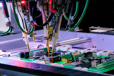
 Image 1: RF PCB Design
Special Offer: Get $100 off your order!
Email [email protected] to get started!
Basic Design Concepts of RF PCBs
1. Impedance Matching
Impedance matching ensures maximum power transfer and minimizes signal loss in RF circuits. Use this table to choose a suitable technique based on your application.
| Impedance Matching Techniques | Description | Application |
| Transmission Line Stubs | Short circuit stubs at precise lengths to adjust impedance | Narrowband circuits |
| Quarter-Wave Transformers | Sections of transmission line one-quarter wavelength long | Single frequency signals |
| Balun Transformers | Convert balanced to unbalanced signals, ensuring compatibility | Antennas |
| Lumped Element Matching | Uses discrete components like capacitors and inductors to tune impedance | Broadband circuits |
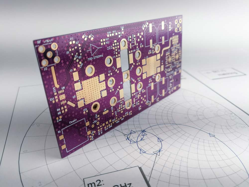
A high-power radio-frequency PCB on a Smith chart for impedance matching and tuning
2. Material Selection
Select materials based on dielectric constant and loss tangent to optimize signal integrity for your frequency range.
| Material | Dielectric Constant (εr) | Loss Tangent | Applications |
| FR4 | 4.5 | 0.02 | Low-frequency RF |
| Rogers | 2.2 – 3.0 | 0.001 – 0.004 | High-frequency, Microwave |
| Taconic | 2.3 – 2.9 | 0.002 – 0.005 | Microwave, High-speed digital |
| Arlon | 2.17 – 3.8 | 0.0018 – 0.004 | High-power RF, Military |
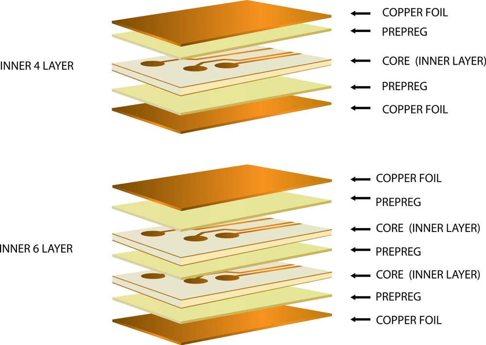
3. Stack-Up Design
A well-designed PCB stack-up is essential to control electromagnetic interference (EMI) and ensure signal integrity. Use this table to select the best configuration.
| Stack-Up Configuration | Description | Benefit |
| Symmetrical Stack-Up | Even layer distribution across the PCB | Prevents warping |
| Ground Plane Below RF Layer | Direct ground path beneath RF traces | Reduces EMI and crosstalk |
| 4-Layer Stack-Up | RF on top, ground plane, power plane, non-RF components | Suitable for small RF boards |
| 6-Layer Stack-Up | Additional signal integrity with two ground planes | Ideal for complex RF systems |
4. Trace Design
Trace design impacts signal integrity. Use the following table to optimize your trace geometry and layout.
| Design Factor | Optimal Approach | Impact on Performance |
| Trace Width | Wider traces lower impedance | Reduced signal loss |
| Trace Separation | Increase spacing between traces | Avoids crosstalk |
| Via Size | Minimize via diameter | Less signal disruption |
| Trace Length | Shorter traces | Minimizes signal attenuation |
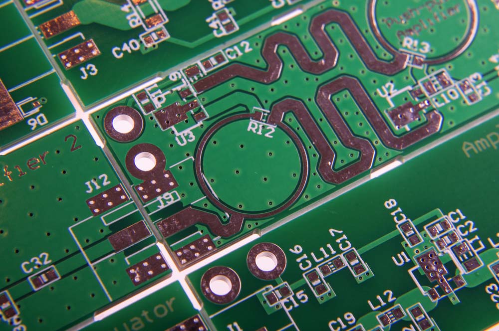
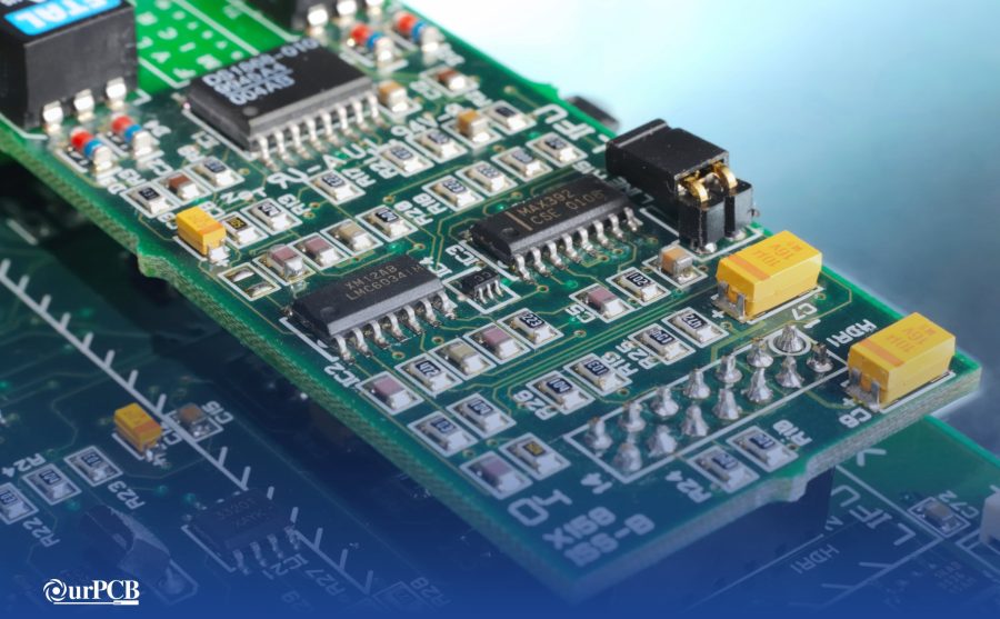
A radio frequency PCB with curved traces
5. Grounding and Shielding
Grounding and shielding prevent noise and interference. Use these techniques for robust designs.
- Ground Plane Design: Utilize continuous ground planes for the shortest return paths, shielding the RF signals.
- Shielding: Apply copper enclosures or add shielding layers to block external noise sources.
6. Thermal Management
Managing heat from high-power RF components is essential to prevent overheating.
| Thermal Technique | Description | Benefit |
| Copper Foil Thickness | Increase copper thickness | Enhances heat dissipation |
| Thermal Vias | Use vias to transfer heat to ground planes | Avoids component overheating |
7. Power Supply Decoupling
Decoupling power supplies reduces noise interference with RF signals.
| Capacitor Type | Placement | Noise Filtered |
| X Capacitors | Across power lines | High-frequency noise |
| Y Capacitors | Between ground and power | Low-frequency noise |
8. Antenna and Component Placement
Correct component placement is critical for maintaining signal integrity. Follow these guidelines:
- Antenna Size: Larger antennas capture more signal but must be placed away from noise sources like digital components.
Component Grouping: Group RF components close together to minimize high-frequency trace length and avoid signal loss.
Key Differences from Standard PCB Designs
RF PCB designs differ from standard PCBs in several key ways. They prioritize signal integrity for high-frequency signals, require precise impedance control, use specialized low-loss substrates, and feature carefully planned layer stack-ups. These design elements are crucial for maintaining signal quality, preventing reflections, supporting high-frequency operations, and managing electromagnetic interference in RF circuits.
Common Issues and Challenges with RF PCB Design
RF PCB design presents several common challenges. Impedance matching is a critical issue, as achieving precise impedance levels can be difficult due to variations in materials and manufacturing tolerances. Crosstalk is another significant concern, where high-frequency signals can interfere with each other if not properly isolated. Additionally, noise reduction is essential for clean signal transmission, requiring designers to minimize electromagnetic interference (EMI) from both external sources and internal components.
Software Tools for RF PCB Design
Recommended Software
- Altium Designer: Offers comprehensive RF design features, including impedance calculators and simulation tools.
- Cadence: Provides advanced RF/microwave design capabilities with extensive simulation options.
- KiCad: An open-source alternative with growing support for RF PCB design, suitable for smaller projects.
Features for RF/Microwave Applications
- S-Parameter Analysis: Allows for the simulation of high-frequency signal behavior.
- EM Simulation: Helps in predicting electromagnetic interference and optimizing shielding.
- Impedance Control Tools: Facilitate the design of controlled impedance traces and matching networks.
Back to Top: RF PCB Design
Special Offer: Get $100 off your order!
Email [email protected] to get started!