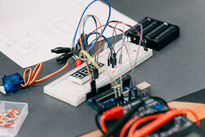
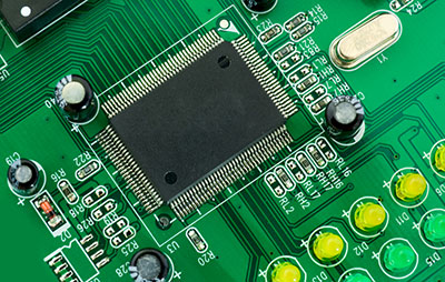
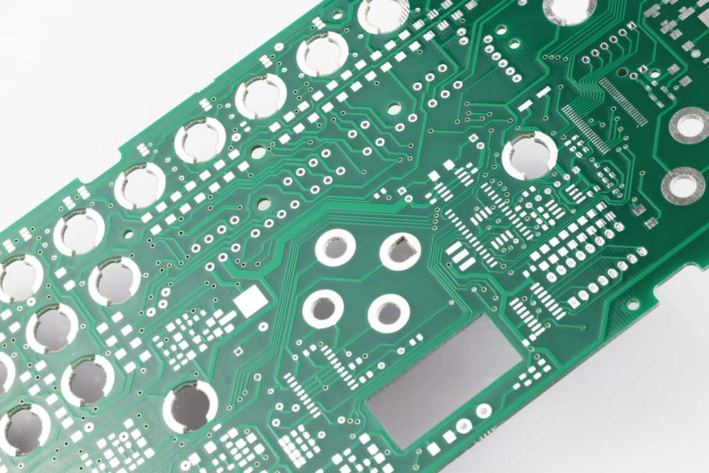
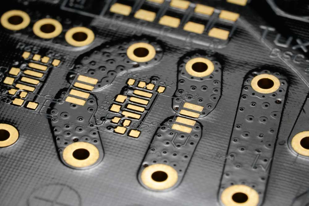
PCB is a multi-floor construction with various passages and links between two or more adjacent floors. As complex as it sounds, designing and implementing a multilayer PCB is a very complicated process. PCB via or vertical interconnection access connects two points that are located on different layers of the PCB. Vias pass current on various electronic devices; for instance, the integrated circuit uses embedded vias surrounded by SiO2 to link between two substrates. PCB via size is the critical feature in the multilayer PCB. Via construction consists of three major components, a metal-plated hole, solder pads on either side, and insulation, and clearance along the entire via.
Special Offer: Get $100 off your order!
Email [email protected] to get started!
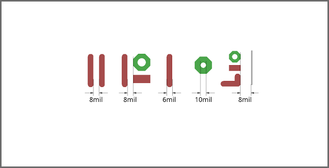
1.PCB via Types
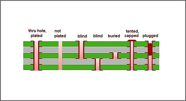
PCB vias are classified into three different types. Through-hole vias, blind via and buried via. As the name implies, each class is classified based on its location on a printed circuit board. Through-hole connects the top and bottom layers of the PCB by cutting through the inner layers. These types of vias are usually the cheapest and easy to construct type as it only needs a plated through-hole, either driller or laser cut. Blind via is typically located on the sides to separate them for the rest of the tracks as it mostly connects power and ground rails to the inner layers. Buried via is embedded into the PCB as it combines the two internal layer points. It is very delicate to drill the Z-axis holes for blind and buried via.
2.Standard PCB via size
As vias are holes, most of the manufacturers can handle any of the standard drill sizes. But it is important to note that the production process will be efficient if all the vias on the boards are of the same size. This will make the drilling process more comfortable and saves considerable time, thus saving production costs. Vias from drills start from 0.15mm with a 0.3mm solder pad and can drill as big as requested, but different sizes may require manual drilling, which increases the production cost. Holes smaller than 0.15mm can only be drilled by laser drill. Via with a 0.6mm hole and a 1mm solder pad is the most common size that can be fud on most PCBs.
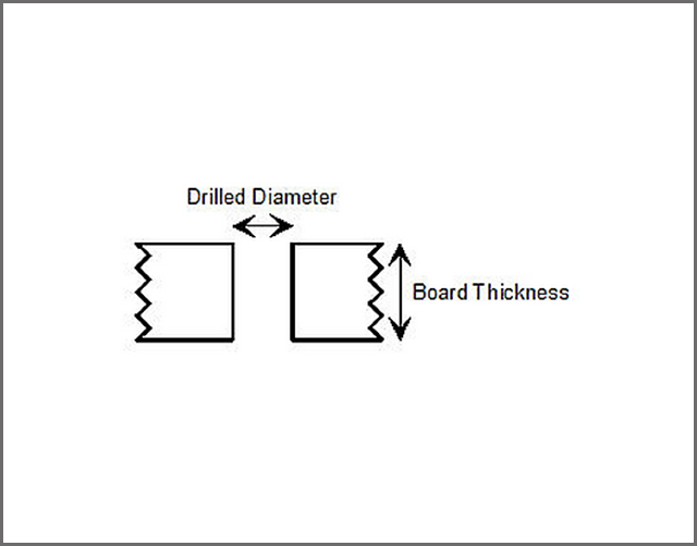
3.PCB Aspect Ratio

PCB’s aspect ratio can be defined as the ratio between the thickness of the board and the diameter of the drilled hole. A balance of 6:1 or more must be achieved to dub the process as efficient. The rate determines the surface area of the hole and the current capacity of the via.
Special Offer: Get $100 off your order!
Email [email protected] to get started!