What does a hex inverter do, and how do they fit into PCBs? These components play a big role in many modern digital components; without them, many of the digital appliances we take for granted wouldn’t work the same way.
OurPCB’s circuit board experts have shared their knowledge to create this guide to hex inverters so you can learn more! We’ll explore the fundamentals of hex inverters, their operational principles, benefits in PCB design, and best practices for their layout and routing.
Contents
- What is a Hex Inverter?
- How does a Hex Inverter Work?
- Benefits of Using Hex Inverters in PCB Design
- Performance and Reliability
- Power Efficiency
- Integration with Other Components
- Types of Hex Inverters
- Common Hex Inverter Models
- CMOS vs. TTL Hex Inverters
- Choosing a Hex Inverter
- Applications of Hex Inverters
- Digital Circuits
- Specific Applications
- Example Circuits Using Hex Inverters
- Voltage Level Shifting with CD4069
- Debounce Circuit Using SN74HC04
- Design Considerations for PCB Manufacturers
- Incorporating Hex Inverters
- Best Practices for Layout and Routing
- Hex Inverter FAQs
- How do you Test a Hex Inverter IC to Ensure It Is Working Correctly?
- Can Hex Inverters Be Used in Analog Signal Processing?
- What’s the Difference Between Hex Inverters and Hex Buffers?
What is a Hex Inverter?
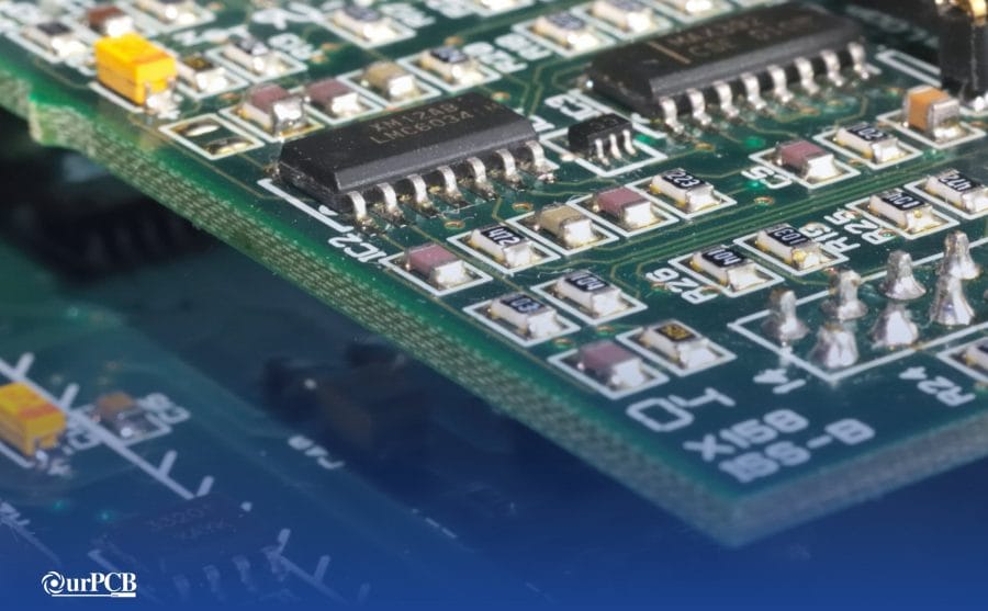
A hex inverter is an integrated circuit (IC) that contains six independent inverter gates. Each inverter gate takes a digital input and outputs the opposite logic level. For example, if the input is high (logic level 1), the output will be low (logic level 0), and vice versa.
Hex inverters are commonly used in digital electronics for signal inversion, logic level conversion, and generating clock signals. One of the most widely used hex inverters is the 7404 IC, which is part of the 7400 series of logic chips.
How does a Hex Inverter Work?
A hex inverter works by using each of its six inverter gates to flip the input signal’s logic level. When a low voltage (0V) is applied to the input of one of the inverters, it outputs a high voltage (typically 5V).
On the other hand, when a high voltage is applied, the output is low. This basic function can be implemented using different technologies, such as NMOS, PMOS, or CMOS transistors.
In practical applications, hex inverters are used for various purposes. They can clean up noisy signals, generate clock signals, and act as buffers to strengthen weak signals. The 7404 hex inverter IC, for instance, is known for its low power consumption and high-speed switching, which makes it suitable for a wide range of digital applications.
Benefits of Using Hex Inverters in PCB Design
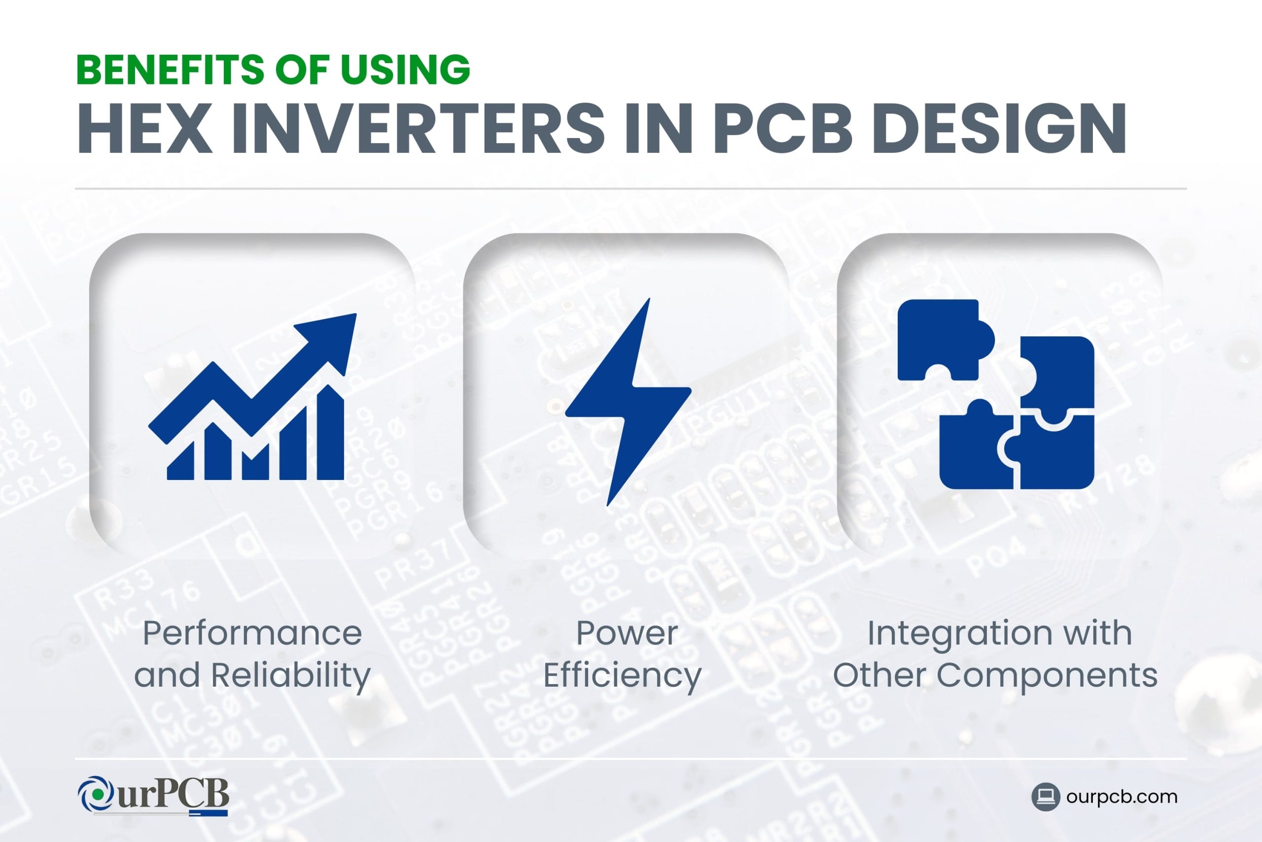
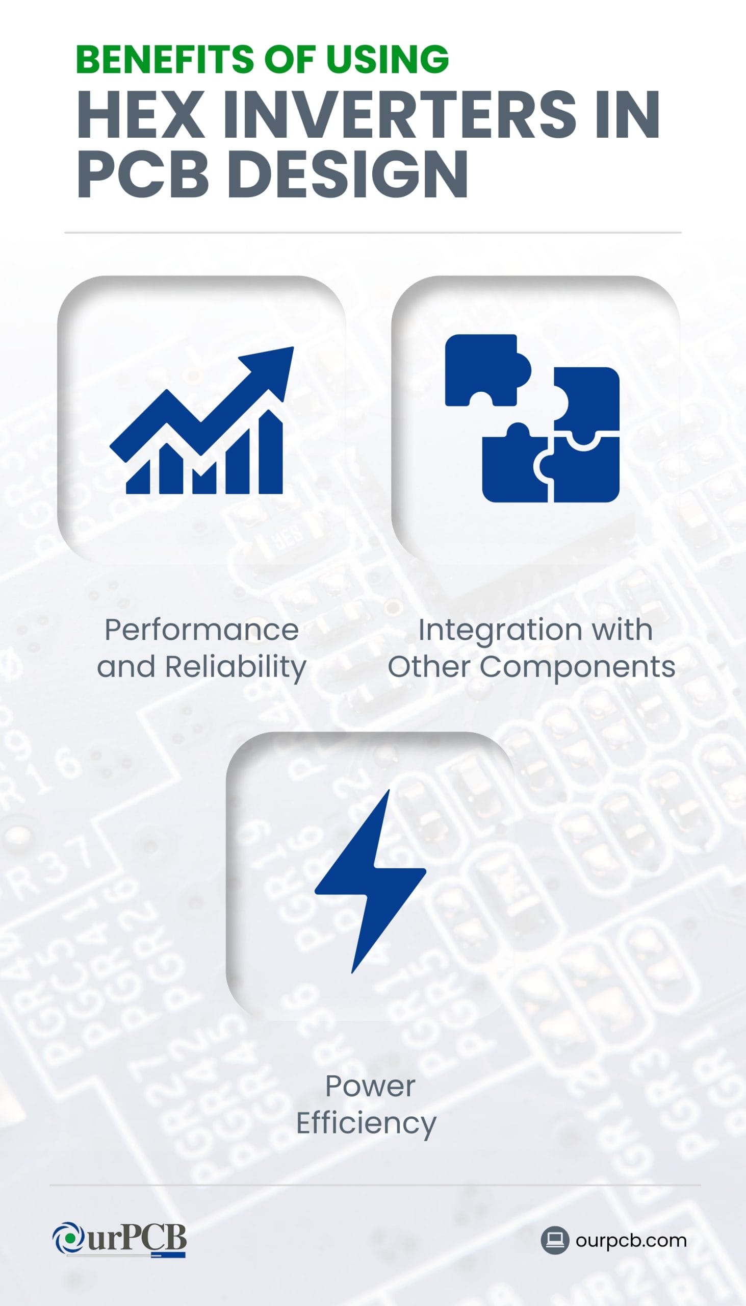
Performance and Reliability
Hex inverters are known for their high performance and reliability in PCB design. These components offer fast switching times and consistent performance, making them ideal for digital signal processing.
They’re capable of handling a wide range of voltage levels, which enhances their versatility in different circuit designs. Also, hex inverters are built to be robust against noise and interference, which maintains stable operation even in less-than-ideal conditions. This reliability reduces the likelihood of circuit failures.
Power Efficiency
Hex inverters are designed to be power-efficient components. They consume minimal power when in non-switching state, contributing to overall energy savings in a circuit. This efficiency is particularly beneficial in battery-powered devices, to avoid draining batteries unnecessarily.
The low power consumption also lowers heat generation, which can boost the longevity and stability of the entire PCB. Inverters like the 74HC04 have low static and dynamic power dissipation, which helps when designing circuits that need prolonged operation without the power draining too fast.
Integration with Other Components
Hex inverters integrate seamlessly with a wide range of other components, making them highly versatile in PCB design. They can be used along with other logic gates, microcontrollers, and sensors to create complex logic circuits.
Their standardized pin configurations and compatibility with various voltage levels simplify the design process, and enables easy incorporation into existing circuit designs. This compatibility extends to both analog and digital circuits, so they are great in mixed-signal applications.
Special Offer: Get $100 off your order!
Email sales@ourpcb.net to get started!
Types of Hex Inverters
Common Hex Inverter Models
Some of the most common models, found in digital electronics, include:
- 74HC04: This is a high-speed CMOS hex inverter with a voltage range of 2 to 6V. It features low power consumption and is widely used in general digital logic applications.
- 74LS04: A TTL hex inverter, known for its fast switching times and compatibility with other TTL logic families. It operates with a 5V supply voltage and is used in applications requiring quick signal inversion.
- CD4069: A CMOS hex inverter with a wide supply voltage range of 3 to 15V. It’s appreciated for its high noise immunity and stable operation across multiple conditions.
- 74HCT04: This model combines the speed of TTL with the low power consumption of CMOS. It has a supply voltage range of 4.5 to 5.5V and is TTL compatible, making it suitable for interfacing with TTL circuits.
CMOS vs. TTL Hex Inverters
Hex inverters can be constructed using different technologies, primarily CMOS and TTL. OurPCB’s team has summarized the key features and specific characteristics of each below:
| Feature | CMOS Hex Inverters | TTL Hex Inverters |
|---|---|---|
| Technology | Uses complementary MOSFET transistors | Uses bipolar junction transistors (BJTs) |
| Power Consumption | Typically, lower consumption than TTL as only one transistor is on at any time | Higher consumption than CMOS due to continuous current flow through the resistive paths |
| Voltage Range | Operates over a broader voltage range (e.g., 3–15V for CD4069) | Typically operates at a fixed voltage (5V) |
| Noise Immunity | — Higher noise immunity compared to TTL — Suitable for environments with higher electrical noise | Can be designed to address low noise immunity |
| Speed | — Modern CMOS inverters can be very fast — Traditionally slower switching times compared to TTL | — Faster switching times in general — Ideal for high-speed digital applications |
Your final decision on CMOS or TTL hex inverters will depend on the specific requirements of the application, including power efficiency, speed, and environmental conditions.
Choosing a Hex Inverter
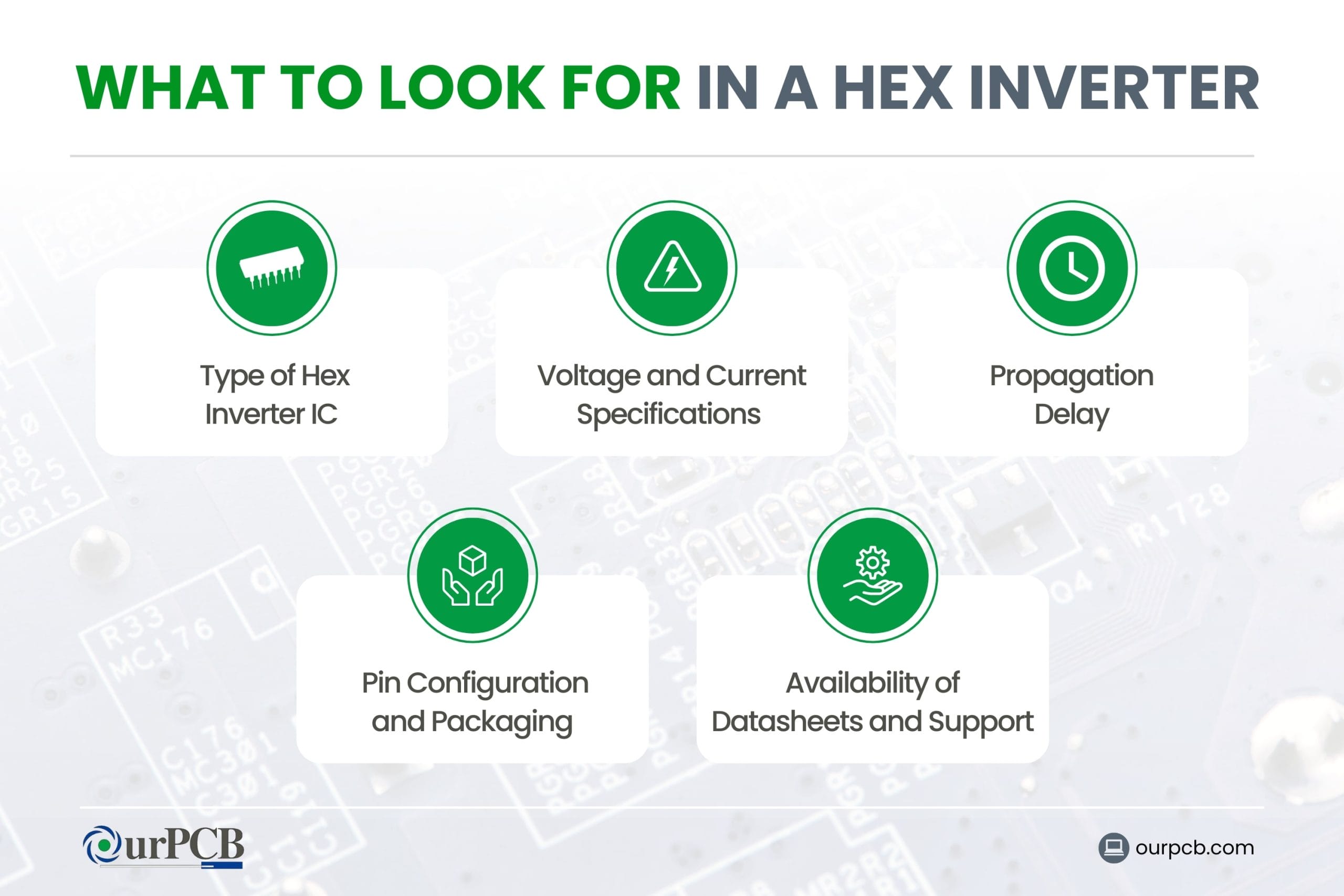
When choosing a hex inverter, it’s important to do your research to make sure you select the right component for your needs. Here are some important aspects to consider:
1. Type of Hex Inverter IC
Hex inverters come in several types, each with unique features which make them suitable for different applications. Common types include:
- 74HC04: Known for high speed and low power consumption, suitable for general digital applications.
- CD4069: Offers high noise immunity and is often used in analog and digital circuits.
- 74HCT04: High-speed CMOS IC with Schmitt trigger inputs for noise-resistant signal processing.
2. Voltage and Current Specifications
Verify that the hex inverter IC matches your circuit’s voltage and current requirements. For example:
- 74HC04: Operates within a voltage range of 2 to 6V and can handle output currents up to 5.2mA.
- CD4069: Can operate between 3 and 18V, making it versatile for various power supplies.
3. Propagation Delay
Propagation delay is the time it takes for an input signal change to produce a corresponding output change. Lower propagation delay is a must for high-speed applications.
4. Pin Configuration and Packaging
Check the pin configuration to make sure it’s compatible with your circuit design. Hex inverters are available in different packages such as Dual Inline Package (DIP), Small Outline Integrated Circuit (SOIC), and Thin Shrink Small Outline Package (TSSOP).
5. Availability of Datasheets and Support
Access to comprehensive datasheets and support documents will help you understand the detailed specifications and usage for the hex inverter. Make sure you have access to these resources before making a purchase.
Applications of Hex Inverters
- Signal inversion
- Clock signal generation
- Square wave generation
- Buffering
- Level shifting between different logic families
Digital Circuits
- Logic gates
- Memory devices
- Signal processing
Specific Applications
- Clock signal generation and buffering (74HCT04)
- Synchronizing inverted clock inputs (SN74HC04)
- Debouncing switches
- Inverting digital signals
Example Circuits Using Hex Inverters
Voltage Level Shifting with CD4069
The CD4069 hex inverter is commonly used for voltage level shifting, which is essential when interfacing components that operate at different voltage levels. In a typical application, the CD4069 can convert a signal from a lower voltage to a higher voltage using a simple resistor-transistor circuit.
This setup often involves connecting the input signal to the gate of an NMOS transistor, with a pull-up resistor connected to the higher voltage rail. When the input is low, the NMOS transistor is off, which allows the pull-up resistor to bring the output to the higher voltage.
Conversely, when the input is high, the NMOS transistor conducts, pulling the output to ground. This hex inverter circuit is effective for shifting signals between different voltage domains while maintaining low power consumption and high noise immunity.
Debounce Circuit Using SN74HC04
A debounce circuit with the SN74HC04 hex inverter is used to eliminate noise and ensure stable digital signals from mechanical switches. When a switch is pressed or released, it can produce multiple transitions due to mechanical vibrations, known as “bouncing.”
The SN74HC04 can clean up these signals by using one of its inverters to invert the noisy signal. This inverted signal is then fed into a resistor-capacitor (RC) network to filter out the noise.
The filtered signal is then passed through another inverter to restore the original logic level, but without the noise. This setup ensures that only a clean, single transition is detected for each press or release of the switch.
Design Considerations for PCB Manufacturers
Incorporating Hex Inverters
When incorporating hex inverters into a PCB design, here are some important factors to consider:
- Power Supply Decoupling: Proper power supply decoupling minimizes noise and keeps the hex inverter stable. Place decoupling capacitors (typically 0.1μF ceramic capacitors) close to the VCC and GND pins of the hex inverter ICs.
- Input and Output Loading: Make sure the hex inverter can handle the required load. Check the datasheet for maximum load capacitance and output current specifications.
- Unused Inputs: Tie unused inputs to VCC or GND to prevent floating inputs, which can cause unstable operation and increased power consumption. This ensures that all inputs are at a defined logic level.
- Trace Length and Layout: Minimize the trace lengths for signal lines to reduce noise and signal degradation. Avoid sharp bends and use proper routing techniques. A solid ground plane can help in reducing electromagnetic interference (EMI).
- Propagation Delays: Consider the propagation delays of hex inverters, especially in high-speed digital circuits. Make sure the timing of your circuit accounts for these delays to avoid race conditions and timing errors.
Best Practices for Layout and Routing
Effective PCB layout and routing will maintain the performance and reliability of circuits incorporating hex inverters. Here are some best practices:
- Ground Plane: Use a continuous ground plane to provide a low-impedance return path for signals. This helps reduce noise and improve signal integrity.
- Power Distribution: Make sure that power distribution is robust. Use wide traces for power and ground lines to minimize voltage drops and provide stable power to all components.
- Trace Width and Spacing: Use appropriate trace widths based on current requirements and spacing to prevent crosstalk and signal interference. Follow industry standards for trace spacing.
- Thermal Management: Hex inverters, especially TTL types, can generate heat. Provide enough copper area for heat dissipation, and consider thermal vias if necessary.
- Signal Integrity: Pay attention to signal integrity by keeping high-speed signals as short as possible. Moreover, avoid crossing signal lines over split ground planes. Use controlled impedance traces for high-speed signals.
- EMI Considerations: To reduce EMI, use proper decoupling, maintain a solid ground plane, and avoid long parallel signal runs. Shielding and proper placement of components can also help mitigate EMI issues.
- Component Placement: Place hex inverters close to the components they interface with to minimize trace lengths and reduce potential signal degradation.
Hex Inverter FAQs
How do you Test a Hex Inverter IC to Ensure It Is Working Correctly?
To test a hex inverter IC, you can use a multimeter to check the output voltage levels in response to known input signals. Applying a known high or low logic level to the input and verifying that the output is the opposite shows that the hex inverter is working. Using an oscilloscope can also allow you to visualize the input and output waveforms to make sure it’s working properly.
Can Hex Inverters Be Used in Analog Signal Processing?
While hex inverters are mainly designed for digital signals, they can be used in analog applications such as waveform shaping and pulse conditioning. However, for purely analog signal inversion, operational amplifiers are usually preferred.
What’s the Difference Between Hex Inverters and Hex Buffers?
Hex inverters invert the input signal (high to low or low to high), while hex buffers amplify the input signal without inversion. Buffers are used to strengthen signals and drive larger loads, and inverters change the logic state of the signal.
Back to Top: Hex Inverter | IC, Chip, Circuit, Logic
Special Offer: Get $100 off your order!
Email sales@ourpcb.net to get started!