As electronic gadgets become tinier to meet consumers' lightweight and mobility requirements, they need micro PCB board to accommodate the electrical circuitry.
However, these gadgets still need to be as capable and reliable as their users expect. So, efficiently designing the microboards is critical to making them functional and reliable.
In this article, we will look at how to design these circuit boards. We’ll cover the recommended micro PCB design guidelines and the challenges of making these microelectronics as well. Let’s start!
Contents
- What Is the Purpose of Micro Circuit Boards
- What Are the Challenges of Microelectronics?
- How To Design Micro PCB Board
- Micro PCB Design Guidelines
- Microvias
- Hole Sizes
- Copper Thickness
- Reliability
- Electrical Testing
- Solder Mask
- Identification Marking
- Security Marking
- Final Finish
- Tips To Create The Smallest PCB
- Applications of Micro Circuit Board
- High Volume, Micro PCB, Ultra Small Size, and Special PCB Supplier: OurPCB Capabilities
- Wrap Up
What Is the Purpose of Micro Circuit Boards
The purpose of micro PCBs is to be the foundation of miniature electronic devices with small form factors.
These boards contain the circuitry that interconnects the electronic components in a tiny and efficient design to form the functional system of the end device.
What Are the Challenges of Microelectronics?
As these modern electronics adopt a smaller form factor and use micro PCBs, they must retain the same or even provide more functionality. Therefore, they must become denser to have the required features.
On the design aspect, this presents the challenge of having a tight pitch between the I/O component connections. The board also requires thin traces with fine spacing in between that do not cause signal interference.
While designing these thin traces, it is important to remember that they should be sufficient to transmit the signal to the other end without losses.
Multilayer designs are necessary in these microelectronics. They enable you to design traces with the required thickness, place them in different layers then interconnect them using different via types or plated-through holes.
How To Design Micro PCB Board
To create fine lines for the micro PCB design, try to implement thin traces with a small line width. These should not present any issue for a regular circuit unless it transmits high current levels. In this case, the traces should be wider.
This will help to reduce the line resistance that can affect signal transmission and cause unnecessary heating.
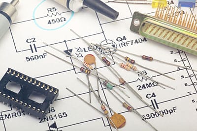
Most designers begin with traces that are 200 microns wide. However, micro PCBs require 13-25 micron-wide aluminum or gold wires (round) to link the silicon die to the chip carrier.
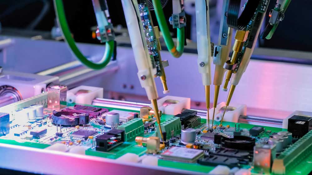
An integrated circuit die wired directly to a PCB
These traces are not strong enough to handle physical abuse and can be dislodged using a solder mask. So, they are usually locked inside the inner layers. Fabricators have also come up with new methods to adhere the copper surface to the PCB to prevent dislodging.
Since micro PCBs are usually multilayer, via holes are essential. To use less surface real estate, you should design microvias that are tinier than the traces. They should also have a smaller annular ring.
Overall, a micro PCB utilizing 3-mil vias, 30-micron lines, and 30-micron spaces creates a 0.2mm pitch layout. This is five times smaller than a regular PCB design.
Special Offer: Get $100 off your order!
Email sales@ourpcb.net to get started!
Micro PCB Design Guidelines
Microvias
These plated hole structures are critical in interconnecting the thin copper layers in the multilayer micro PCB structure.
If you use mechanical drilling, you can make the holes 5.9 mils in diameter and 60 mils thick.
But laser drilling is more precise because it can create holes with a diameter of 2-3 mils and a thickness of 2-4 mils.
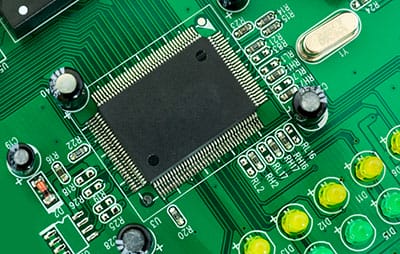
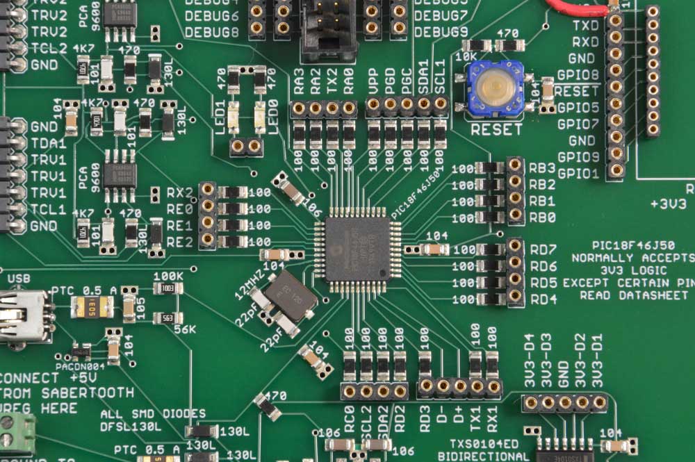
A close-up image of a micro PCB
The surface pad size should match the hole size, which varies depending on the drilling process. Laser-drilled microvias can have a 5-mil pad for a 3-mil microvia, while a 6-mil drilled hole should have a significantly larger 12-mil pad.
Hole Sizes
When creating the layout, it is important to note that you should shrink all the elements of a traditional PCB. This includes the holes. Resizing goes further into the manufacturing process, so you should always inquire if your fabricator can create laser holes (microvias). These are the most suitable for the small form-factor boards to make them functional and optimal.
Copper Thickness
3-mil transmission lines usually require about one ounce of copper. But the microcircuits in micro PCBs need traces about 30 microns (1.18 mils) wide. Manufacturing them involves using pattern plating, meaning the traces don’t have to exit the circuit to a plating bus line. On the other hand, wire bonding plating can either be electroless or electrical.
Reliability
Manufacturers can build micro PCBs with high component densities using the laminates used on regular circuit boards. Most use rigid FR4 laminates, which should be thin and allow the drilling of micro holes or vias.
Electrical Testing
Rigid and flying probe testing methods have a 2-3 mil pitch on the lower limit. This is larger than the pitch of the connectors on the micro PCB. In this case, you should extend the lines from the circuit to a 3-4 mil pad to enable electrical testing after manufacturing.
PCB testing using flying probes
Solder Mask
Although imaging improvements have made it possible for manufacturers to fabricate thin 30-micron lines, this technology has not yet advanced enough on the solder mask application side.
The imaging resolution’s lower limit for solder masks is stuck at the 75-micron position accuracy.
Identification Marking
Regular silkscreen identification markings and images are also too large for micro PCBs. But you can use a very fine inkjet printer to create the small markings for the small form factor circuit.
Silkscreen markings on a PCB
Security Marking
These markings are usually tiny barcodes on the solder mask that can be invisible to the human eye. They help identify the PCB for purposes like traceability.
Final Finish
Like regular PCBs, micro-circuit boards require surface finishes to protect the exposed copper surfaces. However, most rely on three finishes: immersion tin, immersion silver, and bondable soft gold.
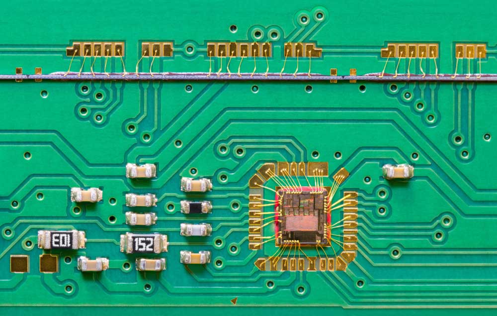
Micro PCB Board: A PCB with a gold surface finish (ENIG)
Tips To Create The Smallest PCB
Designing the tiniest PCB assembly manufacturing unit requires considering the lowest possible limits of all manufacturing elements. This includes the silkscreen width, text size for markings, solder mask clearance, trace width, and the minimum clearance for the solder mask, vias, solder paste, holes, and surface finishes.
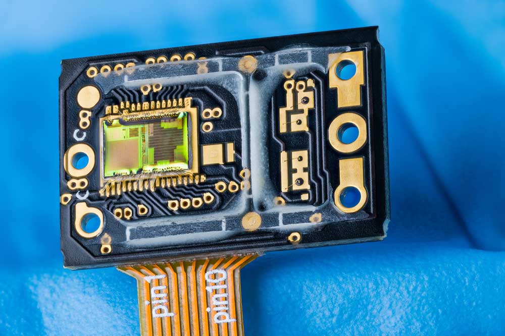
Micro PCB Board: An optoelectronic image sensor PCB with a green silicon die
Vias are equally important in this equation for interconnecting the multilayered structure, and we recommend using blind and buried vias.
These structures will greatly maximize the routing space, making it possible to make the board as tiny as possible.
Buried vias are particularly important because they don’t reach the surface, meaning you’ll have extra real estate.
Also, leave some space between the components to enable trace routing. Avoid components with multiple pins as well because they require more space. Proper spacing simplifies soldering as well.
Applications of Micro Circuit Board
PCB miniaturization has become the norm in various industries as manufacturers embrace integrated circuit chips.
You can find them in power electronics, RF and high-speed digital circuits, LEDs, semiconductors, instrumentation devices, industrial and contract manufacturing services, etc.
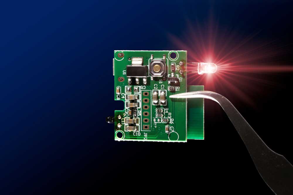
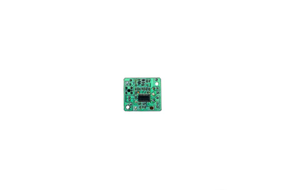
Micro PCB Board: A tiny microcontroller PCB with an infrared LED
High Volume, Micro PCB, Ultra Small Size, and Special PCB Supplier: OurPCB Capabilities
When selecting your micro PCB manufacturer, you need to pick a partner who can address the challenges of micro PCB fabrication and help you meet the board’s design guidelines.
At OurPCB, we are capable of these and provide single-point source manufacturing where we source all the materials and then build your micro PCB with a rapid turnaround time.
We can build boards that have up to 50 layers with 0.1 mil buried and blind vias. You can pick the substrate material from a wide selection and we’ll deliver the complete PCB in 5-6 days (can be expedited to 24-48 hours).
We also do PCB assembly in-house and perform various reliability tests, such as flying probe, solderability, impedance, and hole resistance testing. Check out our full list of capabilities here.
Wrap Up
Designing and manufacturing micro PCBs is challenging, but you can trust us to do the manufacturing and assembly after you handle the design part.
Before we begin fabricating the PCB, we'll do a full design-rule check to ensure the layout has no issues. If we spot problems, we’ll share them with you and help you sort them out as soon as possible. Our goal is to actualize your circuit design in the shortest time possible.
Contact us today with your design files, and we’ll give you a free quote for the batch you need.
Special Offer: Get $100 off your order!
Email sales@ourpcb.net to get started!