In this article, we’re going to dive into the definition of schematic diagrams, what the purpose of the schematic diagram is, what does a schematic diagram show, and more.
At OurPCB, we have the capabilities to assess your schematics and work from there, or help you with designing a PCB schematic diagram.
Let’s define schematic diagrams for you.
Contents
- What Is A Schematic Diagram?
- What are the Different Types of Schematic Diagrams?
- Circuit Schematics
- Block Diagrams
- Wiring Diagrams
- Logic Diagrams
- Common Schematic Diagram Symbols
- How to Read Schematic Diagrams
- Identify the Symbols
- Follow the Connections
- Read the Labels
- Understand the Power Supply
- Use Reference Designators
- Practice with Simple Circuits
- Why are Schematic Diagrams Important?
- Clear Communication
- Troubleshooting and Maintenance
- Efficient Design Documentation
- Safety
- What is the Standard Specification for PCB Schematics?
- IEC60617
- ANSI Standard Y32
- How Do You Create a Schematic Diagram?
- Step 1: Define the Purpose
- Step 2: Set Up Your Schematic Design Environment
- Step 3: Add Component Libraries
- Step 4: Place Components
- Step 5: Draw Connections
- Step 6: Add Ports and Power Connections
- Step 7: Annotate the Schematic
- Step 8: Review and Verify
- Rules to Remember for Drawing Schematic Diagrams
- What are the Benefits of Using a Schematic Diagram Tool?
- Clear and Organized Diagrams
- Extensive Component Libraries
- Circuit Simulation Features
- Time-Saving
- How to Avoid Common Mistakes
- Plan Your Layout
- Use Consistent Naming
- Check Pin Configurations
- Proper Placement of Decoupling Capacitors
- Verify Component Footprints
- Don’t Rely on Automatic Routing
- Use Built-In Checks
- OurPCB: Simplified Schematic Diagrams
- Schematic Diagram FAQs
- Are there any free schematic diagram tools available?
- Can you modify an existing schematic diagram?
- What is the difference between schematic and wiring diagrams?
What Is A Schematic Diagram?
What is schematic diagram in electronics? A schematic diagram is a visual representation of an electrical circuit or system. It uses symbols to show each component and its various connections. These schematics drawings help engineers, electricians, and technicians understand how a specific system works. Schematics for a PCB are extremely helpful for complicated systems.
What are the Different Types of Schematic Diagrams?
The main types of schematic diagrams include circuit schematics, block diagrams, wiring diagrams, and logic diagrams. Each of these schematic image types serves a unique purpose in electrical and electronic design. Understanding the different types of schematic diagrams will help you select the right diagram schematic form for a specific task.
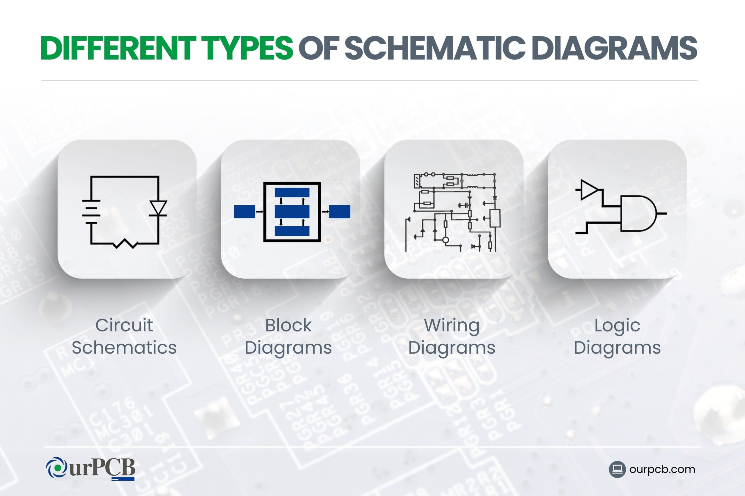
Circuit Schematics
Circuit schematics are detailed diagrams that show the exact connections and components in an electrical circuit. This system schematic model provides a clear map of how electricity flows through the system, making it easier to spot problems and understand how the circuit works.
Block Diagrams
Block diagrams are a simplified overview of a system. Instead of showing detailed connections, they use labeled blocks to represent entire components or sections of a circuit.
These diagrams provide a “big-picture view” of a system’s design. They help show how different parts of a system interact without getting bogged down in the details.
Wiring Diagrams
Wiring diagrams focus on the physical layout of wires and components. They show how everything is connected in real life, often using realistic pictures or simple drawings in machine schematics.
Logic Diagrams
Logic diagrams are used in digital electronics to show how different logic gates and circuits interact. They use symbols to represent different types of gates, like AND, OR, and NOT gates. They provide a clear way to see how inputs are processed to produce outputs.
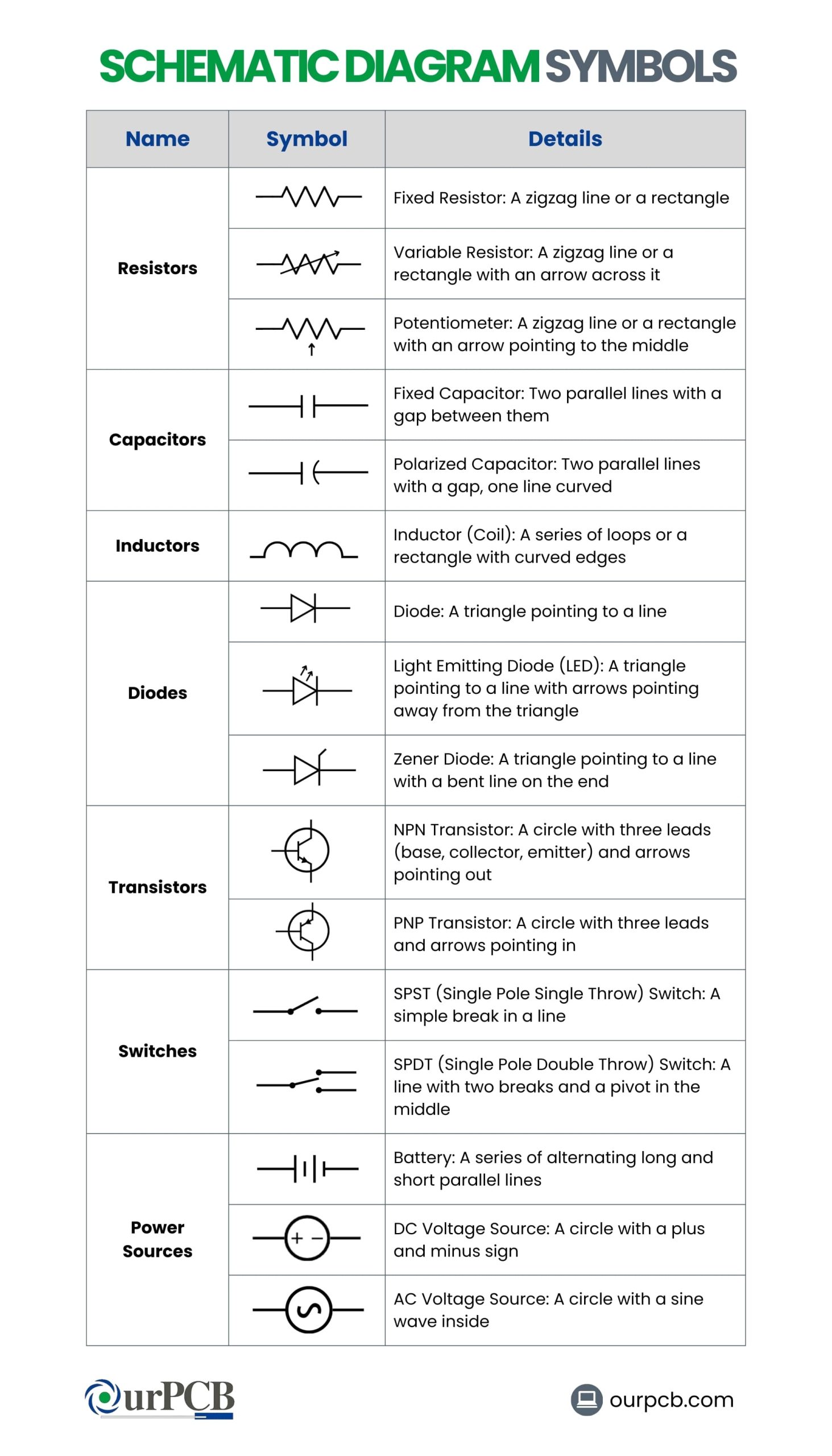
Common Schematic Diagram Symbols
How to Read Schematic Diagrams
Most schematic diagrams are made up of basic symbols. Learning how to read PCB schematic diagrams is important for anyone working with electronics. Here’s how schematic analysis works:
Identify the Symbols
Each component in a PCB schematic diagram is represented by a unique schematic symbol. For example:
- Resistors: Shown as zigzag lines or rectangles
- Capacitors: Depicted as parallel lines (with a curved line for polarized capacitors)
- Inductors: Look like coiled wires or squiggly lines
- Diodes: Have a triangle pointing to a line
- Transistors: Represented with three terminals labeled base, collector, and emitter for BJTs, or gate, drain, and source for MOSFETs
Follow the Connections
Components are connected by lines representing wires. These lines show how current flows through the circuit:
- Nodes: Points where wires connect, usually marked by dots
- Junctions: Where two or more wires meet
- Crossings: Without a dot, meaning the wires do not connect
Tracing these connections helps you see the path of electricity through the circuit.
Read the Labels
Labels provide important information about the components and their values:
- Resistor values: Indicated in ohms (Ω)
- Capacitor values: Given in farads (F), often microfarads (μF) or picofarads (pF)
- Voltage and current ratings: Specified for various components
These labels help you understand the specifications and requirements of each part.
Understand the Power Supply
Every circuit needs a power source. Look for symbols that indicate the power supply, usually shown as:
- VCC or +: For positive voltage
- GND: Or ground for the negative terminal
Knowing where the power enters the circuit is important for understanding its operation.
Use Reference Designators
Each component is usually labeled with a reference designator (R1, C1, Q1, etc.), which helps you identify the components on the actual PCB:
- R: For resistors
- C: For capacitors
- Q: For transistors
These designators match the parts list or bill of materials (BOM) that comes with the schematic.
Practice with Simple Circuits
Start by reading simple schematics to build your skills. As you become more familiar with the symbols and connections, move on to more complex diagrams. Practice will improve your ability to quickly and accurately interpret PCB schematics.
Why are Schematic Diagrams Important?
Now that we’ve broken down the meaning of schematic diagrams, let’s get into why they’re necessary. Here are a few reasons why a schematic diagram important.
Clear Communication
Schematic diagrams provide a clear and standardized way to explain complex electrical circuits. By using universally recognized symbols and layouts in a schematics diagram, it’s easier for engineers, technicians, and electricians to understand the workings of a circuit without confusion.
Troubleshooting and Maintenance
When a problem arises in an electrical system, schematic graphs or diagrams are particularly helpful for troubleshooting. They help technicians find issues quickly by following the diagram to see where things might have gone wrong. This saves time and reduces the chances of errors.
Efficient Design Documentation
Creating a schematic drawing or diagram helps in planning the layout, choosing the most suitable parts, and making sure everything fits together correctly. Once the design is finished, the schematic serves as a detailed blueprint for building the system.
Safety
Schematics show how components should be connected to prevent dangers like short circuits or electrical fires. Electricians can install systems correctly and safely based on electrical schematic plots designs.
Special Offer: Get $100 off your order!
Email [email protected] to get started!
What is the Standard Specification for PCB Schematics?
The standardization of schematic notation, including PCB schematics, is governed by two international standards.
IEC60617
The IEC 60617 standard, published by the International Electrotechnical Commission (IEC), includes over 1,750 symbols for schematic diagrams.
ANSI Standard Y32
The ANSI Standard Y32, provided by the American National Standards Institute (ANSI), includes specialized notations that were first used in aircraft applications. This standard has been updated to align with IEC 60617, and it’s mainly used in the United States.
How Do You Create a Schematic Diagram?
Creating a schematic diagram involves several steps that make sure your diagram is clear, accurate, and useful. Here’s a step-by-step guide to help you with schematic diagramming.

Step 1: Define the Purpose
Before starting, think about the goal of your schematic diagram. Are you designing a new circuit, documenting an existing one, or troubleshooting? Knowing the purpose will guide you through the entire process.
Step 2: Set Up Your Schematic Design Environment
Begin by opening a new project in your chosen PCB design software like Altium Designer, KiCad, or Eagle. Once your project is set up, create a new schematic file. This will be the workspace where you design your circuit.
Step 3: Add Component Libraries
Next, you need to add component libraries to your design tool. These libraries contain the symbols and footprints for all the electronic components you’ll use. Many design tools come with built-in libraries, but you can also download others.
Step 4: Place Components
Start by placing the central components of your circuit. Add other components, like resistors, capacitors, and connectors, around the main IC. Each component should be labeled with a reference designator (e.g., R1 for the first resistor).
Step 5: Draw Connections
Connect the components using lines that represent electrical wires. Follow standard conventions: power and ground connections should be clearly marked, and signals should be labeled to show their function. Use a grid to align components and connections neatly.
Step 6: Add Ports and Power Connections
Add ports for inputs and outputs to show where signals enter or leave the circuit. Include power and ground symbols to indicate how the circuit is powered. These will help anyone who reads the schematic understand the flow of electricity through the schematic.
Step 7: Annotate the Schematic
Add annotations to provide extra information about the circuit. This might include notes on component values, specific part numbers, or any special instructions for assembly. Detailed notes can help others understand your PCB design.
Step 8: Review and Verify
Before finalizing your schematic, review it for errors. Most PCB design software includes tools for electrical rule checking (ERC) and design rule checking (DRC) to identify potential issues, like unconnected pins or incorrect component values.
Rules to Remember for Drawing Schematic Diagrams
- Lines for Electrical Connections: Use lines to show electrical connections. Add a node (dot) if intersecting lines are connected
- Limit Node Connections: Ideally, connect only three lines to a single node for clarity
- Use Named Nets: Name nets in complex circuits. Nets with the same name are connected, even if not directly linked.
- Horizontal Text: Write pin numbers, polarity indicators, values, and net names horizontally
- Input and Output Placement: Place inputs on the left and outputs on the right
- Functional Blocks: Group components into functional blocks based on their roles in the circuit
- Pin Number Placement: Place pin numbers outside the symbol graphics
- Sheet Connection Symbols: Put sheet connection symbols on the far left or right edges of the page
- Title Block: Position the title block in the lower right corner of the first sheet; include title, part number, and revision details
What are the Benefits of Using a Schematic Diagram Tool?
There are tons of advantages of using a schematic for engineers, electricians, technicians, and more. Let’s get into a few benefits of using a schematic diagram tool.
Clear and Organized Diagrams
Schematic diagram tools make complex systems simpler by breaking them down into smaller, more manageable parts. This helps users see how different components connect and work together, making it easier to understand and troubleshoot circuits.
Extensive Component Libraries
These tools usually have vast libraries of electronic components, such as resistors, capacitors, and transistors. This makes it easy to find and use the right parts in your design, helping you maintain accuracy and consistency.
Circuit Simulation Features
Many schematic tools include simulation capabilities that allow you to test and validate your designs before building them. This helps identify and fix potential issues early, saving time and resources.
Time-Saving
Schematic diagram tools also come with built-in symbols and shapes, which speed up the process of creating diagrams. This allows you to focus on design rather than spending time drawing each component manually.
How to Avoid Common Mistakes
Creating a schematic diagram can be complex, and mistakes are easy to make. Here are some tips to help you avoid common errors when you create your schematic map or diagram:
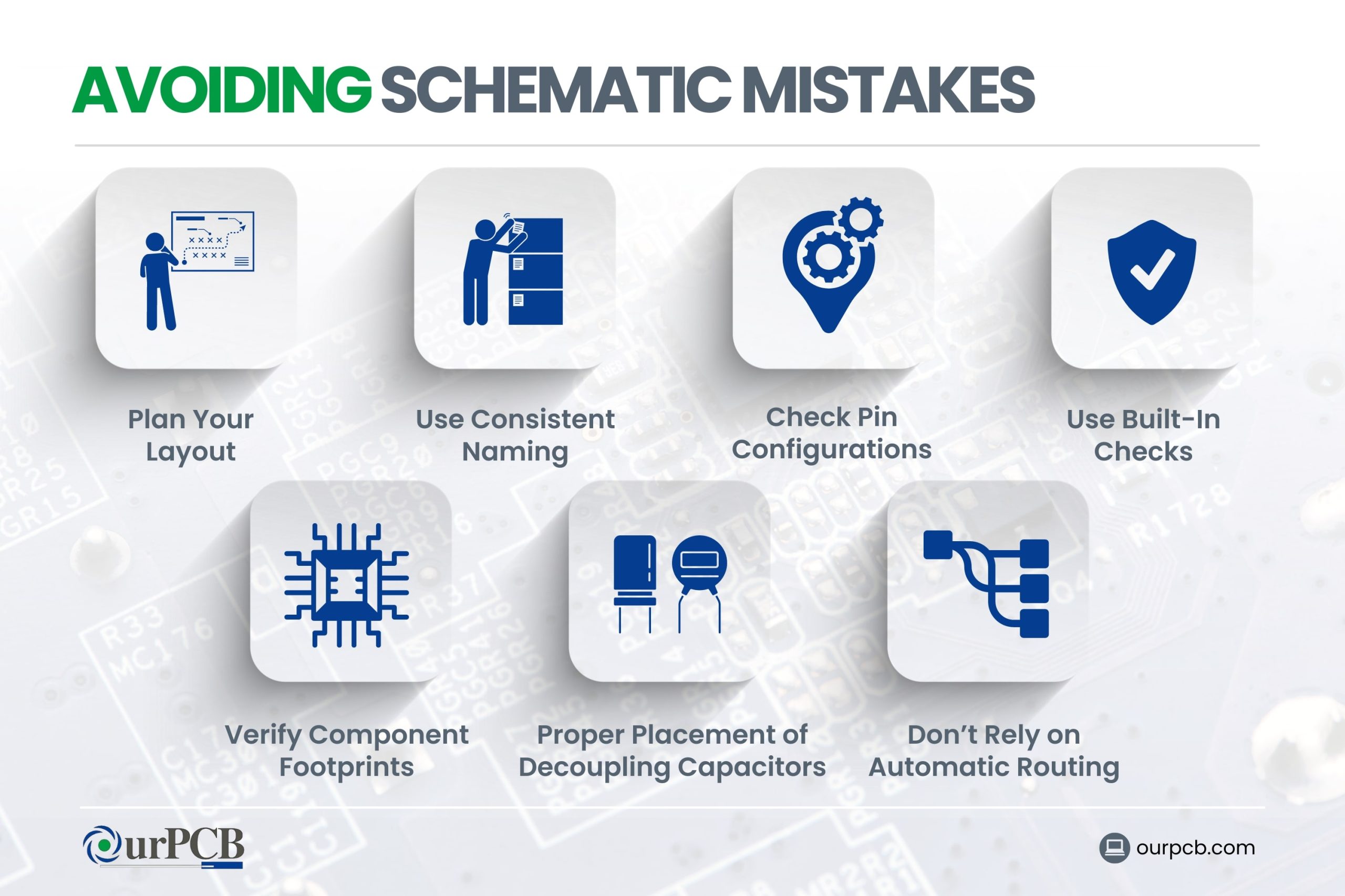
Plan Your Layout
One of the most common design mistakes in schematic design is poor layout planning. Start by organizing your components logically. Place related components near each other and plan the flow of your design from input to output. This makes your schematic easier to read and reduces the chance of connection errors. Additionally, consider heat-generating components early in the design phase, as effective PCB Thermal Management strategies must be incorporated from the schematic stage to ensure optimal performance.
Use Consistent Naming
Make sure that each voltage and ground net has a consistent name throughout your schematic. Inconsistent naming when drawing schematics can lead to faulty connections and errors in the final design. Double-check that all power and ground connections are correctly labeled and connected.
Check Pin Configurations
For programmable devices, double-check that the pin configurations match the requirements of your PCB layout. Mixing up input and output pins can cause issues. Be sure to communicate with your design team early to confirm pin configurations and power requirements.
Proper Placement of Decoupling Capacitors
Place decoupling capacitors as close as possible to the power pins of the components they are meant to support. This maintains a stable power supply and reduces noise and oscillations in your circuit.
Verify Component Footprints
Make sure that the footprints (landing patterns) of your components match the specifications. Incorrect pad sizes or spacing can cause alignment issues during soldering, leading to faulty connections. Always refer to the component datasheet to verify the correct footprint.
Don’t Rely on Automatic Routing
While automatic routing can save time, it may not always produce the best results. Manual routing allows for better control over trace paths, reducing unnecessary vias and optimizing space. Use automatic routing as a starting point, but review and adjust the routing manually for best results.
Use Built-In Checks
Many schematic design tools have built-in checks to identify errors. Use these tools to verify connections, check for unconnected pins, and make sure all components are properly placed and connected. Regularly run these checks throughout the design process to catch mistakes early.
OurPCB: Simplified Schematic Diagrams
A schematic diagram is really useful visual representation of an electrical circuit or system. With simple symbols and labels, you can easily understand how a system works.
There are various types of schematic diagrams that are useful for different projects. Make sure to follow our simple rules to avoid common mistakes when creating a schematic design, and you’re good to go!
If you need a little help designing a PCB schematic diagram, you are more than welcome to reach out. We’ll be happy to take your project from idea to reality!
Schematic Diagram FAQs
Are there any free schematic diagram tools available?
Yes, free schematic diagram tools like KiCad, Scheme-it by DigiKey, and Fritzing are available. KiCad supports schematic capture and PCB design, Scheme-it offers an online platform with a comprehensive symbol library, and Fritzing provides an easy-to-use interface for beginners.
Can you modify an existing schematic diagram?
Yes, you can modify an existing schematic diagram using various design tools. If you need help modifying a diagram, or you’re unsure how to, contact OurPCB — we’d be happy to help!
What is the difference between schematic and wiring diagrams?
In schematic diagrams, you use lines to show different wires, and symbols to indicate different components, while wiring diagrams are a simpler visual representation of an electrical circuit. The components in a wiring diagrams are shown using basic shapes, but they tend to offer more information about the location and positioning of your devices.
Back to top: Schematic Diagram
Special Offer: Get $100 off your order!
Email [email protected] to get started!