

Why Apple Manufactures in China (And What Hardware Startups Can Learn From Its Playbook)
When asked why Apple manufactures in China, ‘cheap labor’ is the facile answer. The more accurate one is supply chain engineering. A modern iPhone may
 5 Star Rating on
 OurPCB manufactures high-reliability single-sided PCBs for OEMs and electronics manufacturers that require stable, consistent circuit board performance across industrial, automotive, medical, and communications sectors.


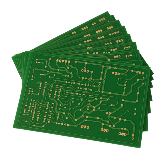

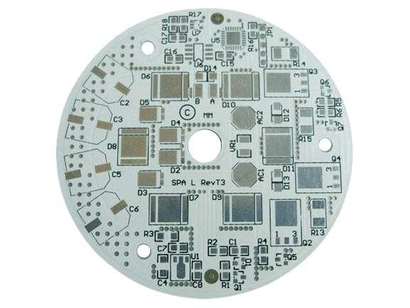
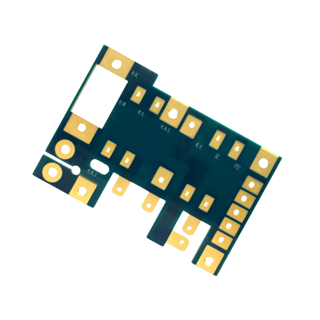
OurPCB manufactures single-sided PCBs focusing on mechanical stability, electrical reliability, and precise adherence to client specifications. Each PCB is built on a single substrate layer, supporting a conductive copper layer on one side of the board. Our single-sided printed circuit boards serve industries that require durable, low-cost circuit solutions, including industrial automation, automotive subsystems, medical measurement devices, and consumer electronics.
Our PCB manufacturing process uses high-quality base materials such as FR4, High TG FR4 halogen-free, and CEM-3, selected based on thermal, mechanical, and environmental operating conditions. Surface treatments such as solder mask application and ENIG (Electroless Nickel Immersion Gold) finishing enhance the durability and solderability of every PCB board. Each printed circuit board is inspected against IPC-A-610 Class 2 or Class 3 standards to validate trace width, copper integrity, and conductor spacing, delivering high-quality single sided solutions for volume production or prototype needs.
A single-sided PCB is a type of PCB built with one layer of conductive copper laminated onto a substrate material. First introduced commercially in the 1950s, single-sided PCBs simplified early electronics manufacturing by allowing all conductive paths to be placed on one surface. This single layer PCB structure allows for simplified routing, reduced manufacturing cost, and mechanical rigidity suited for various applications.
The production process for a single sided printed circuit board involves applying a thin copper sheet to a dielectric substrate, patterning the circuit layout through a photo-imageable process, and applying a protective solder mask to shield exposed traces.
The copper layer is laminated using heat and adhesive systems to achieve strong adhesion between the substrate and the conductive material. As a basic type of PCB, single-sided designs eliminate the need for via interconnections, reducing manufacturing complexity and improving yield for high-volume production.
Single-sided boards are manufactured with copper weights ranging from 0.5 to 3 oz per square foot, depending on current carrying and mechanical strength requirements. Material selection, including FR4, High TG FR4, or CEM-3, impacts thermal resistance, dielectric strength, and board rigidity based on the operating environment.
Having only one conductive layer minimizes signal integrity challenges such as crosstalk and interlayer noise, although heat dissipation and limited routing density must be carefully considered in the PCB design phase.


Single-sided PCBs are widely used in industries where circuit simplicity, cost control, and mechanical durability are more important than multilayer complexity. Single sided PCB assembly manufacturers provide printed circuit boards for:

In consumer electronics, single-sided PCBs are used in calculators, audio amplifiers, remote controls, and small appliance circuits. These PCB boards require minimal routing complexity and benefit from the mechanical stability and low production cost of a single layer solution.
Standard FR4 substrates combined with automated wave soldering processes make high-volume production fast and reliable for everyday electronics.
Industrial systems use single sided circuit boards in control panels, sensor modules, motor drives, and measurement devices. The conductive copper traces support moderate current loads and resist mechanical shock, making this type of PCB ideal for robust operating environments.
In applications exposed to higher temperatures, High TG FR4 or CEM-3 materials provide better thermal resistance and longer service life under load.
Automotive applications integrate single sided PCBs into lighting systems, dashboard controls, mirror adjusters, and actuator controllers. The PCB must withstand vibration, thermal cycling, and moisture exposure while maintaining reliable circuit performance with one layer of conductive copper.
FR4 materials with optional ROHS-compliant solder finishes meet automotive reliability and environmental standards.
LED lighting modules and compact power supply units rely on single-sided printed circuit boards to handle current distribution, voltage regulation, and thermal dissipation. A high copper thickness and precision solder mask finish ensure electrical integrity and consistent performance in enclosed or high-heat installations.
For high-frequency LED drivers and converters, optional Rogers substrates support lower dielectric loss and improved thermal transfer properties.

We manufacture single-sided PCBs using high-resolution imaging and chemical etching processes to achieve trace widths and spacing down to 2.5 mils. The circuit layout accuracy supports optimized signal flow, minimal resistance paths, and uniform current distribution across the PCB board.
Fine feature patterning is verified under IPC-A-610 and IPC-6012 criteria to ensure that single-sided printed circuit boards meet mechanical and electrical tolerance requirements critical for assembly and performance, supporting higher circuit reliability and reducing signal integrity issues under load.
Our fabrication process includes the application of protective solder masks with thicknesses between 15 and 25 microns, depending on board type and environment. Optional surface finishes such as HASL, ENIG, or OSP are applied to protect exposed pads and enhance solderability.
The solder mask shields copper circuits from oxidation, mechanical abrasion, and solder bridging during reflow or wave assembly. Surface finish choice is tailored based on product shelf life, soldering method, and environmental exposure conditions.
We select PCB materials such as standard FR4, High TG FR4, CEM-3, and Rogers (preferred for RF applications, they’re also used in LED and high-thermal-load designs) halogen-free laminates depending on thermal, mechanical, and dielectric requirements.
Our team evaluates each substrate for glass transition temperature (Tg, the temperature where the material transitions from rigid to soft), coefficient of thermal expansion (CTE, the rate at which the material expands when heated), dielectric constant (a measure of a material’s ability to store electrical energy), and insulation resistance (the ability of the material to resist electrical leakage under voltage stress).
Our process allows for copper thickness from 0.5 oz to 3 oz, depending on current load and mechanical strength needs. Trace width and spacing are calculated based on amperage flow, thermal rise limits, and allowable voltage drop, ensuring durable conductive pathways across the PCB.
In-process inspections include copper peel strength testing to validate the adhesion between the copper layer and the dielectric base, delivering quality single sided printed circuit structures ready for production deployment.
We inspect each printed circuit board visually at multiple stages to identify etching defects, open circuits, solder mask misalignments, pad contamination, or mechanical damage.
Optical magnification and automated optical inspection (AOI) systems verify fine conductor spacing and pad placement across the entire PCB board surface, minimizing the risk of electrical shorts, open circuits, and misaligned assembly points during downstream PCB assembly.
Bare board testing (BBT) procedures are applied after visual inspection to confirm that the board is electrically sound before component assembly.
Our technicians evaluate solder mask application thickness, coverage uniformity, and adhesion strength, typically achieving between 15 and 25 microns in cured thickness. The soldering process quality is enhanced by verifying that mask windows align precisely with pad locations, preventing solder bridging during reflow or wave soldering.
Silkscreen markings are reviewed for legibility, chemical durability, and positional tolerance under IPC-A-610 guidelines.
All single-sided printed circuit boards undergo 100% electrical continuity testing using flying probe testers or custom-built fixture systems. Open circuits, shorts, and cross-connections are detected and recorded.
Electrical verification follows IPC-6012E standards for bare board electrical testing, confirming that each circuit meets the resistance, open, and short specifications defined in the project documentation.
We perform insulation resistance testing between isolated conductive layers and traces where required, applying controlled high-voltage conditions to detect micro shorts or dielectric failures.
Test voltages and insulation thresholds are set based on IPC-6012E recommendations and customer specifications. This ensures that the substrate material and circuit isolation properties meet critical product safety and performance standards.
Finished boards are measured for length, width, thickness, hole positioning, and mechanical tolerances according to IPC-6012E requirements. Cross-sectional samples verify copper thickness, distribution uniformity, and the presence of any plating voids.
Copper peel strength testing is performed on representative samples, requiring a minimum adhesion of 5 lbs/inch to ensure strong bonding between the copper layer and the underlying dielectric substrate.
Depending on the application, we perform environmental stress tests such as thermal cycling, humidity resistance, and solder shock to validate field performance. Thermal cycling subjects boards to repeated heating and cooling between -40 °C and +125 °C to simulate real-world operating stresses and uncover latent defects such as microcracking or delamination.
Humidity resistance testing exposes completed boards to elevated humidity (up to 85% RH at 85 °C) to verify insulation resistance stability and detect moisture ingress pathways. Solder shock testing rapidly immerses boards in molten solder baths to evaluate pad adhesion, copper layer integrity, and substrate dimensional stability under sudden thermal loads.
OurPCB provides full-service PCB manufacturing and PCB assembly capabilities focused on producing quality single sided solutions that meet strict electrical, mechanical, and thermal performance requirements.
We fabricate single-sided PCBs directly to customer-submitted Gerber files, IPC-2581 packages, or ODB++ data. Trace widths, clearances, pad sizes, solder mask openings, and drill hole specifications are verified before production release.
Circuit board technology processes such as copper balancing, solder mask dam control, and image-to-drill registration are applied to ensure precise feature alignment on every PCB board. Panelization methods, including V-cut scoring and breakaway tabs, are supported for volume production efficiency. Boards are built to meet IPC-A-610 Class 2 or Class 3 acceptance standards, depending on the application.
Our PCB fabrication process supports PCB materials selection based on electrical, mechanical, and thermal demands. Available substrates include standard FR4, High TG FR4, CEM-3, and Rogers laminates, sourced from leading material suppliers such as Rogers Corporation and Shengyi Technology. All base materials comply with IPC-4101 specifications for mechanical, thermal, and dielectric performance.
Finish options include HASL, ENIG, OSP, and immersion silver, matched to client assembly method and environmental storage needs. Copper PCB layers are laminated and etched using chemical and mechanical processes optimized for adhesion, trace integrity, and durability.
We operate modern PCB production lines with direct imaging equipment, solder mask screen printers, automatic optical inspection (AOI) stations, chemical surface finish lines, and X-ray registration verification. Our processes control layer PCB integrity with positional tolerances of ±0.05 mm and copper etch-back within IPC-defined limits.
The minimum mechanical drill size capability is 0.1 mm, allowing precise hole placement even in compact layouts. Solder mask registration is controlled within ±75 microns to ensure proper pad exposure. Maximum panel dimensions up to 450 mm × 600 mm are supported for batch production. For tight-tolerance builds, X-ray drilling verification confirms layer-to-hole alignment accuracy.
In addition to single-sided builds, we manufacture double-sided PCB and flexible PCB products through parallel production lines, allowing streamlined scheduling and integrated quality control.
Internal quality systems are aligned to ISO 9001, IATF 16949, ISO 13485, and IPC-A-610 standards. Our inspection workflow includes solder mask thickness measurement, copper thickness validation, insulation resistance testing, peel strength verification, and dimensional accuracy checks.
Final inspections on every PCB lot confirm compliance with electrical continuity, open/short detection, and mechanical fitment requirements. Production data is archived for traceability, supporting downstream PCB assembly or system integration processes.
Every PCB is fabricated strictly according to client-supplied Gerber files, stackup drawings, and BOM specifications. No material substitutions, pad resizing, or drill reassignments are made without client approval.
If we identify manufacturability risks, DFM (Design for Manufacturability) feedback is provided to the client before production release, maintaining full design ownership and traceability throughout the PCB production cycle.
OurPCB operates under ISO 9001 (quality management), IATF 16949 (automotive quality systems), ISO 13485(medical quality systems), and IPC-A-610/IPC-6012 Class 2 (dedicated service electronics) and Class 3 (high-performance service electronics) certification systems. Each build is serialized or batch-coded for full manufacturing traceability.
Our quality workflows validate copper trace geometry, insulation resistance, peel strength, and overall dimensional accuracy, producing high-quality single sided products ready for industrial, medical, automotive, and consumer applications.
We source PCB materials from globally recognized suppliers, including Shengyi, ITEQ, Panasonic, and Rogers. All substrates, copper foils, and solder masks are certified RoHS and REACH compliant, and halogen-free material options are available where regulatory requirements apply.
This ensures that every printed circuit board manufactured by OurPCB meets both technical and environmental compliance standards.
Our production scheduling allows quick transitions from quotation to delivery. Standard production lead times range from 4 to 25 working days, depending on order complexity.
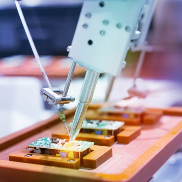
For clients ordering assembly services, in-line SPI (Solder Paste Inspection) and AOI (Automated Optical Inspection) checkpoints are applied during the manufacturing sequence, preserving lot integrity and ensuring downstream assembly success.
Completed PCB boards are packed in ESD-safe materials, labelled with batch numbers and material certifications, and shipped with full inspection reports where required. For prototypes or New Product Introduction (NPI) lots, optional First Article Inspection (FAI) reports are available to document dimensional, material, and electrical compliance against project specifications.
International shipping support includes customs clearance documentation, certificates of origin, and carrier tracking integration for all outbound shipments.
Mon-Fri: 24 hours,
Sat: 9am-6pm, GMT+8
Reach us at
[email protected]
24 hours online
+86-199-30589219
Mon-Fri: 24 hours
Sat: 9am-6pm, GMT+8
Yes. OurPCB supports both prototype and low-volume production for single-sided PCBs, offering flexible lot sizes starting from just one panel. Prototype orders follow the same controlled PCB fabrication processes as full production runs, including full electrical testing and mechanical inspection. Clients receive rapid DFM feedback if needed, ensuring that prototype builds are ready for evaluation and final validation.
Yes. Single-sided PCBs can be designed to handle high-voltage circuits by applying appropriate trace spacing, creepage distance, and material selection practices. For voltages above 100V, wider conductor gaps are applied according to IPC-2221B standards, and high dielectric strength substrates such as High TG FR4 or specialized halogen-free materials are recommended. Protective coatings like thicker solder masks can also be specified to reduce arc risk and environmental degradation.
Our standard copper thickness options for single-sided PCBs include 0.5 oz, 1 oz, 2 oz, and 3 oz per square foot. Thickness selection depends on current-carrying capacity, thermal performance, and mechanical strength requirements.
Copper thickness is validated post-processing by microsection analysis to ensure compliance with IPC-6012 standards, typically within a ±10% tolerance band around the specified nominal value.
OurPCB can fabricate single sided PCB panels up to a maximum finished size of 450 mm × 600 mm. Larger panel sizes allow cost-effective array configurations for small part assemblies or high-volume production runs. Panelization options such as V-cut scoring or tab routing are used to optimize board usage and streamline downstream depaneling during PCB assembly or final product integration.
We offer multiple surface finish options for single sided PCB fabrication, including HASL (Hot Air Solder Leveling), ENIG (Electroless Nickel Immersion Gold), OSP (Organic Solderability Preservative), and immersion silver.
Each finish is selected based on soldering method, storage conditions, product lifecycle expectations, and cost considerations. ENIG is preferred for fine-pitch components requiring flat coplanarity, while OSP offers an economical choice for assemblies built within shorter timeframes.
We offer PCB materials including standard FR4, High TG FR4 for improved thermal performance, CEM-3 for cost-sensitive builds, and Rogers laminates for high-frequency or thermal management applications. Each substrate selection is matched to electrical performance, thermal resistance, dielectric strength, and mechanical durability based on client design and environmental needs.
Proper material selection directly affects electrical insulation strength, mechanical stability under thermal cycling, and overall field reliability of the finished product.
All single-sided printed circuit boards undergo 100% electrical testing based on IPC-9252 guidelines. We use flying probe testers for prototypes and fixture-based test systems for production volumes. Tests verify open circuits, short circuits, and continuity across all conductive pathways. High-voltage insulation resistance tests are also applied when required to confirm dielectric barrier performance between isolated circuits.
Comprehensive electrical testing reduces the risk of latent defects during product deployment and ensures long-term operational safety, particularly in automotive and industrial environments.
Our technical manufacturing teams, certified quality systems, and client-driven production processes ensure that every PCB meets demanding industrial, automotive, medical, and consumer application requirements.
When asked why Apple manufactures in China, ‘cheap labor’ is the facile answer. The more accurate one is supply chain engineering. A modern iPhone may

PCB tariffs from China can significantly change the real cost of a U.S.-bound order before your boards reach production. A quote may look competitive at

Wire harness tariffs from China commonly fall under HTS 8544.30, the U.S. Harmonized Tariff Schedule (HTSUS) classification for ignition and other wiring sets used in

Unverified wire harness suppliers pose significant risks that often surface long after delivery. A weak crimp, wrong insulation material, missing UL rating, or undocumented connector

Placing an initial Purchase Order (PO) with an unverified China-based PCB supplier can critically jeopardize your budget, launch timeline, and product quality. Knowing how to
Underwriters Laboratories (UL) help engineers, buyers, and manufacturers choose wire and cable that can safely perform in specific electrical, mechanical, and environmental settings. These standards
We use cookies to improve your browsing experience, which may include personal information. By clicking "Agree," you accept our Privacy Policy and cookie use. You can change your cookie settings in your browser anytime.
Agree Chat With Us
  Free Quote