Also, the PCB coil works effectively as an onboard planar inductor. In other words, you can replace a physical inductor component with the RF coil. So, it's a great appliance to have because it saves you space and money.
So, in this article, we decided to give you a breakdown of what it is, how to create one, and more.
Let's begin!
Contents
What Is a PCB Coil?
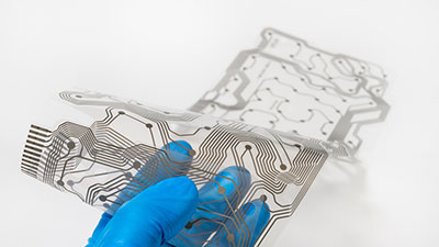
PCB Coil
Source: Wikimedia Commons
The PCB coil is a device that comes from using selected shapes to print metallic traces on a print circuit board. Interestingly, you can execute this process on multiple layers for different shapes and models.
Also, the PCB has some contrasting isolating layers and conductors interwoven to shape the PCB coil collectively in groups.
Further, the device has a conductor layer that comprises a trail. Hence, it fits the suitable bow form and separates into many distinct conductive parts.
Coil PCB in a larger view
Source: Researchgate
In addition, the device has fragments that connect directly to layers. As a result, the PCB will have filaments or power flow patterns. With this, you can calibrate the coil so that each filament gets a significant equal time close to the matched ring.
And the coil's filament moves in a repeated pattern, outwards, upwards, within, and downwards. Consequently, the filaments will contribute to the coil's mutual autonomy transconductance. Also, it's vital to note that all the transistor layers may have related traces and connectors (intralayer).
Special Offer: Get $100 off your order!
Email [email protected] to get started!
PCB Rogowski Coil
PCB Rogowski Coil
Source: Wikimedia Commons
The Rogowski coil is the device you need to calculate the current in a grid over a period. Also, this device is more common than a standard magnetic core current transformer because of its affordability and non-saturation feature.
Also, the device uses an easy production technique, impressive calculation precision, and broad measurement radius.
The drawback of the Rogowski coil is its disparity in phase angle and low reciprocal inductance. But you can fix the gap in the phase angle with an integrated circuit. So, the Rogowski coil effectively measures three-phase current in a circuit breaker space.
Also, the Rogowski coil's low reciprocal inductivity translates to having a low signal-to-noise ratio. But the device is prone to external magnetic field interference. And that's why the Rogowski coil's design comes with an integrated circuit and a large shared inductance.
Specifications of the Rogowski Coil
- Output voltage = 0.023mV/A.
- interference coefficient = 0.26%
- Circuit amplitude = 62.2dB (at the power level)
- Configuration of the circuitry ranges from 50Hz to 1kHz
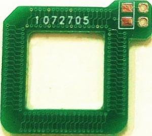
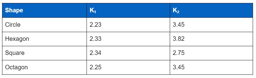
PCB Coil Calculator
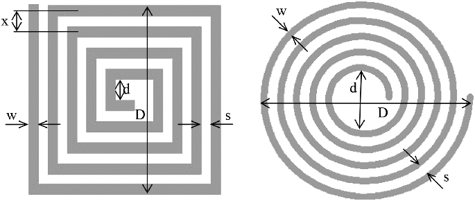
PCB Coil Dimensions
Source: Researchgate ℅ Michal Ulvr
There are three methods you can use to calculate PCB inductors:
First Method
It's based on the modification of H.A Wheeler's expression for inductors (planar spiral).
L = K1µ0 N2Davg/ (1 + K2ɸ)
Where:
ɸ - fill factor
N – number of turns
µ0 – magnetic constant (4π x 10-7)
L – inductance (µH)
Davg – average coil diameter (µm)
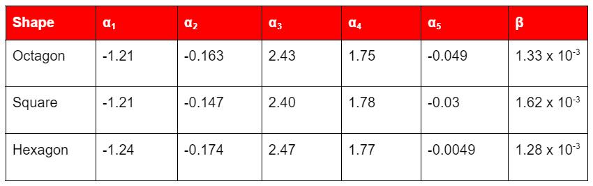
The K1 and K2 coefficients depend on the coil's layout or shape. Here is a summary of different forms:
Second Method
It's a monomial expression. And it came from fitting a significant database of inductors with their exact values.
L = βDα1 Wα2 Dα3avg Nα4 gα5
Where:
g – the gap between the turns (s – W) (µm)
N – number of turns
D – the coil's outer diameter (µm)
L – inductance (µH)
Davg – coil's average diameter
W – PCB trace's width
With that in mind, the coefficients of αi and β depend on the layout you're using. The summary of the coefficient for different formats is as follows:
Third Method
This one is from the electromagnetic principles. All you need to do is estimate the spiral sides.
L = µ0N2Davgc1/2 (In (c2/ɸ) + c3ɸ + c4ɸ2)
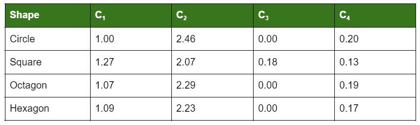
Important Things to Note
The accuracy of the third formula may reduce when the s/W ratio increases. And it shows a maximum error of about 8%. Furthermore, you can build practical integrated spiral inductors with W ≤ s.
That said, you have to define your layout and coil diameter before calculating. So, if your result is beyond the printed trace acceptable size, adjust your diameter. Then, recalculate your coil.
Typically, you should expect about 2 – 3% errors for the three expressions. In addition, if you want to determine the hollowness of your inductor, use the coil's average diameter (Davg) and filling factor (ɸ).
Davg = (D + d)/ 2
ɸ = (D – d)/ (D + d)
Where:
D – coil's outer diameter
d – inner diameter of the coil
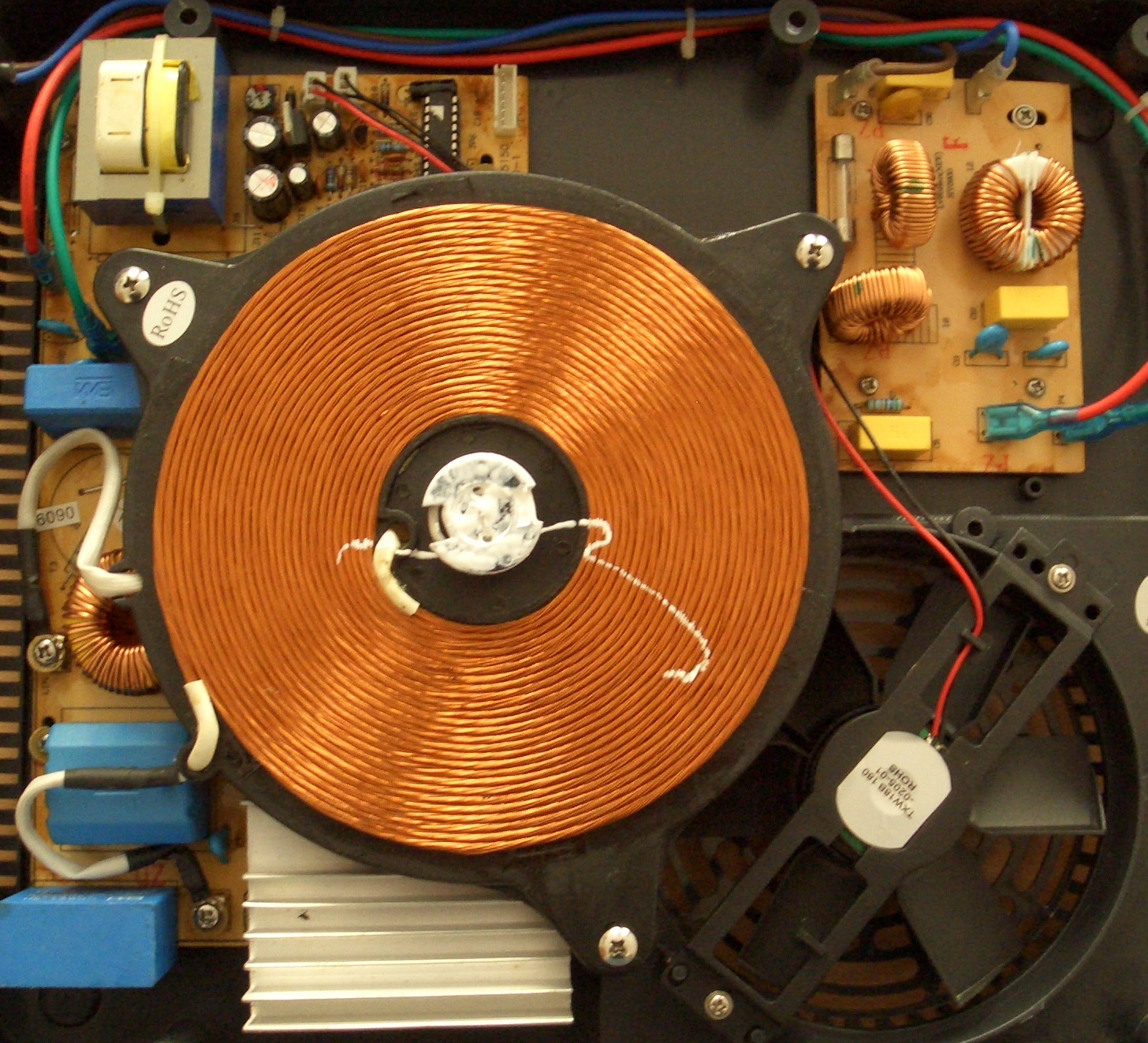
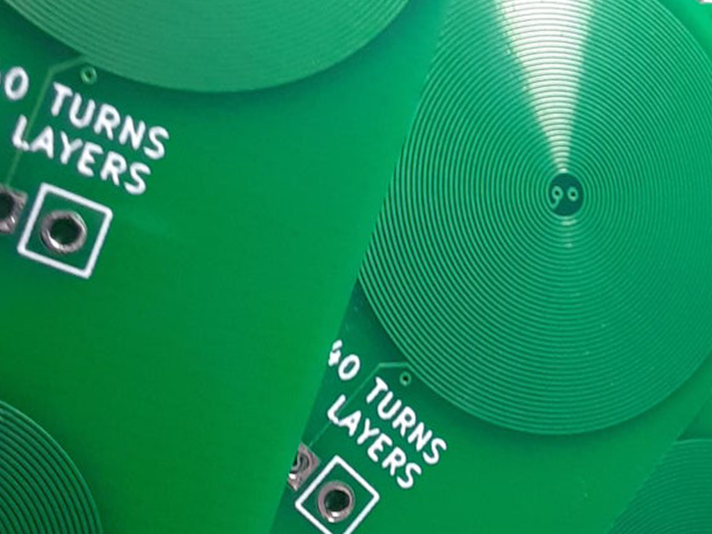
PCB Coils Manufacturing
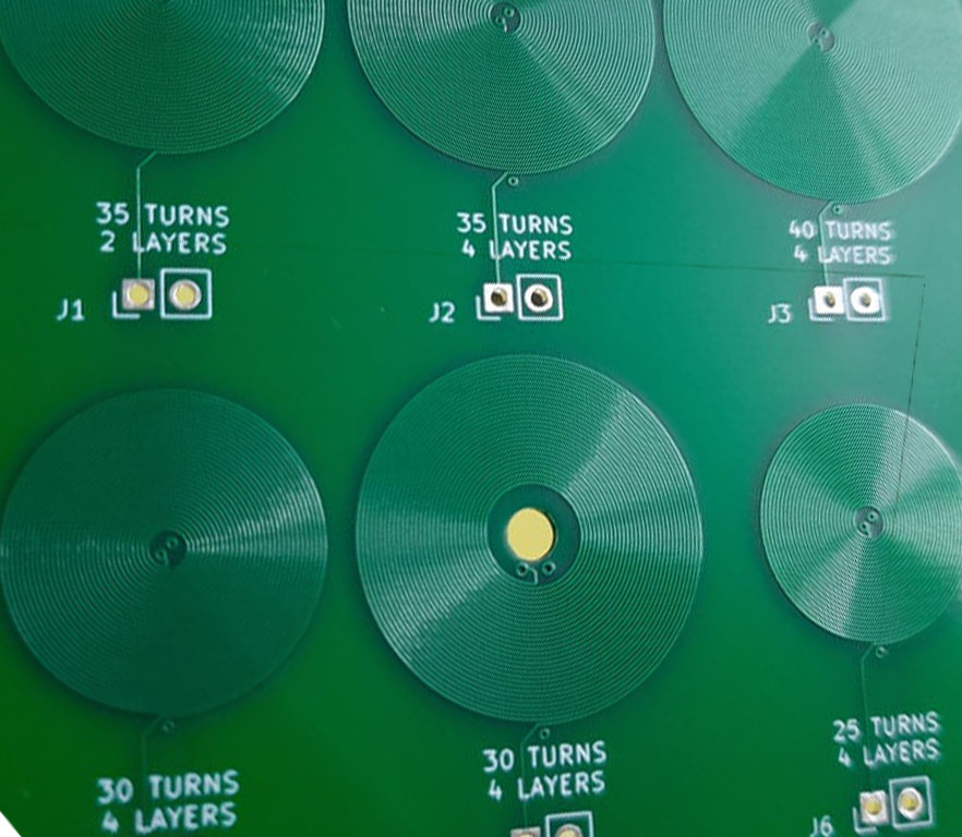
PCB COils on a board
Source: Wikimedia Commons
This section will show how to construct a prototype PCB alongside spiral variants. But before jumping into the project, use a flexible actuator as a guide. In addition, you can use the variations below to get accurate results:
- 40 turns – 4 layers
- 35 turns – 2 layers
- 25 turns – 4 layers
- 30 turns – 4 layers (includes a hole at the core)
- 35 turns – 4 layers
- 30 turns – 4 layers
Step 1
With the variations in mind, put a connector on your motherboard. Then, wire the board in turns. Consequently, your wire becomes a coil on your board. While you're at it, keep the net amount in mind (where the first and second are zero and one, respectively).
At this point, you need to use python code alongside the proper IDE. Then, pick your preferred trace and test the sides. You can start with the radius and follow up with the distance. Also, pay attention to the track spacing. That is, the track spacing should be double the track width.
So, if you have more sides, your coil will be smoother. And you have to set some parameters like rotation path, the number of poles, copper plate, and net number. Afterward, run the script. Then, you'll see a display of numbers in the output pane.
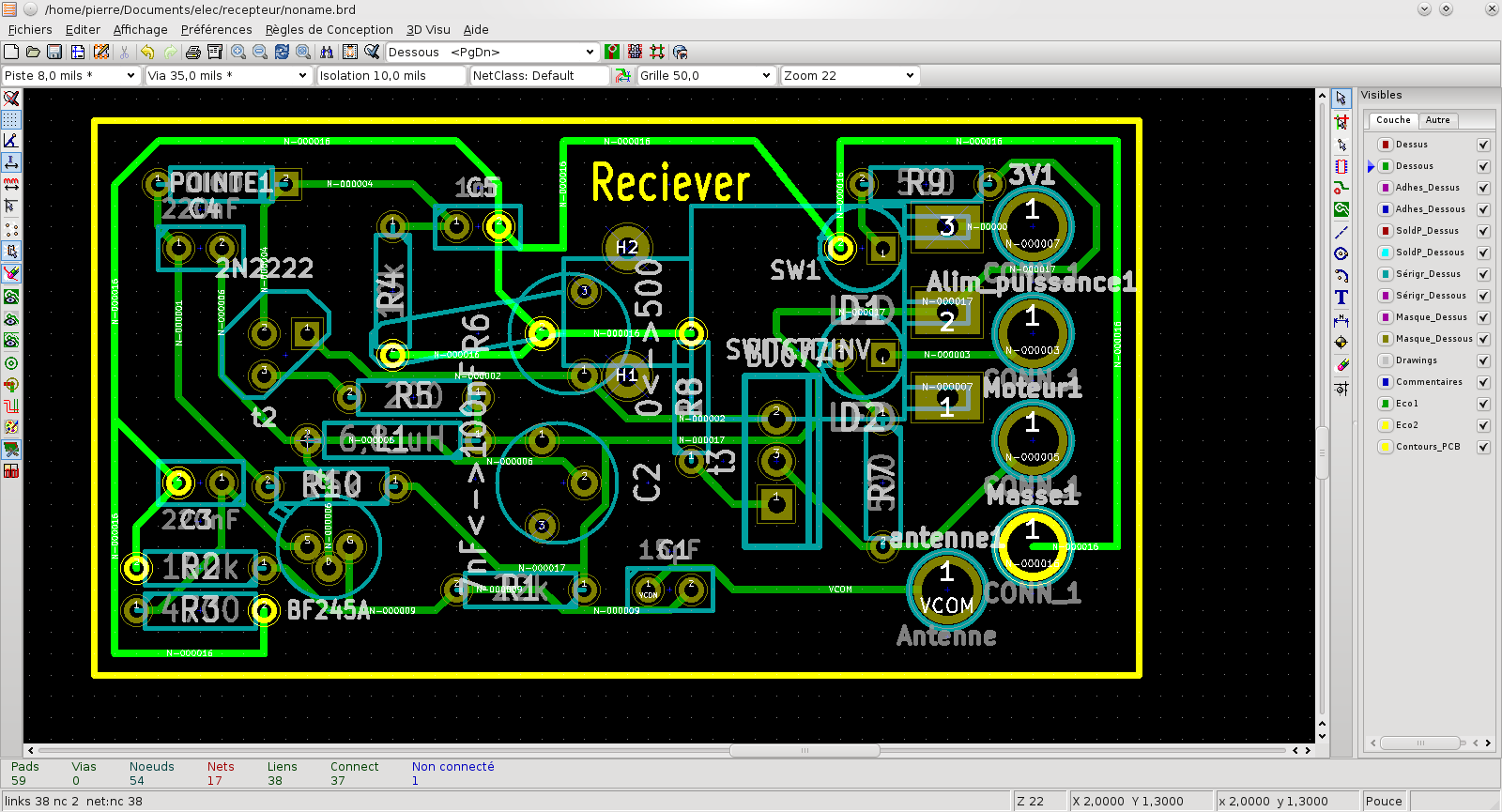
Please copy & paste the figures and save them in PCB format. Then, open your KiCad PCB file to see the coil.
KiCad PCB
Source: Wikimedia Commons
Step 2
Use a thick copper coil PCB to create your coils. In other words, your copper coil can be about 0.13mm thick. When you finish with the PCB design, you can upload the Gerber files to OurPCB and place your order.
Step 3
You can choose to plan and print some fragments in different sizes and shapes at this stage. For instance, if your coil's copper track is 0.13mm, it means that your ring will handle a maximum of 0.3A.
So, the electromagnet for your first construction should be about 1.4A. But you'll have to reduce the force. Also, you have to decrease the wall thickness and section. Then, retain the initial form and measure it with different magnet sizes. That way, your segments will remain lightweight.
Step 4
Finally, you can lift your segments with the 30 turns and four layers variations on each layer. While you're at it, use a neodymium magnet (6 x 1.5mm).
Rounding Up
The PCB coil may have thermal issues. But the pros outweigh the cons as they are affordable, highly versatile, and easy to fabricate. Also, the PCB coils have strong potential for WPT (wireless power transfer) applications.
And you can improve the device's performance by placing a soft magnetic material amid the coil. Further, if you follow specific design rules, you may have a PCB coil with power efficiency and excellent quality.
Do you need help with building a PCB coil? Or do you need the best one for your project? Please feel free to contact us.
Special Offer: Get $100 off your order!
Email [email protected] to get started!