Contents
- What are the Different Types of HDI PCBs?
- Comparison of HDI PCB Types: Type I to Type VI
- What are the Key Features of HDI PCBs?
- What are the Advantages of HDI PCBs?
- What are the Potential Disadvantages of HDI PCBs?
- HDI PCB Design Considerations
- Materials Matter
- Software is Key
- Talk to the Manufacturer
- Layer Stackup is Crucial
- Trace Design Matters
- Vias are Everywhere
- Component Placement is Key
- Signal Integrity is Everything
- What are the Main HDI Structures?
- Stacked Structure
- Any-Layer Structure
- HDI PCB Manufacturing Process
- Sequential Lamination
- Via Metallization and Filling
- Materials Selection
- Applications of HDI PCBs
- High-Density Interconnect (HDI) PCB Technology FAQs
- What’s the Difference Between HDI and a Traditional PCB?
- Can you Design an HDI PCB by Yourself?
- How Reliable are HDI PCBs?
What are the Different Types of HDI PCBs?
- Type I: This HDI PCB only has a single layer of through-hole and blind vias on one or both sides of the substrate or core material. It has no buried vias.
- Type II: These circuit boards feature through-hole vias and stacked microvias, with some having buried vias filled with conductive or non-conductive paste. These buried vias can also be partially or fully filled with dielectric material from the lamination process.
- Type III: Type III HDI PCBs have through-hole vias and two or more layers of stacked microvias and buried vias. Like with type II HDI PCBs, the buried vias can be prefilled with conductive or non-conductive paste. They can also be partially or fully filled with the laminate’s dielectric material.
- Type IV: This HDI circuit board features a passive substrate with no electrical connections. However, this core can provide CTE, thermal, or shielding functions.
- Type V: Type IV HDI circuit boards are coreless. They have an even number of layers laminated together when the interconnections (microvias and conductive paste) are made between the odd and even layers. This construction does not involve SBU because it is a single lamination process.
- Type VI: This PCB contains alternating constructions of the coreless layer pairs. Fabricators form the mechanical structure and electrical interconnections simultaneously either sequentially or via co-lamination. The conductive interconnections between the layers can be formed using conductive paste, anisotropic paste/film, or dielectric piercing posts.
Comparison of HDI PCB Types: Type I to Type VI
High-Density Interconnect (HDI) PCBs are categorized into different types based on their construction, layer count, and capabilities. Below is an expanded table comparing Type I to Type VI HDI PCBs, highlighting their key features, construction methods, and typical applications.
| Feature | Type I HDI PCB | Type II HDI PCB | Type III HDI PCB | Type IV HDI PCB | Type V HDI PCB | Type VI HDI PCB |
|---|---|---|---|---|---|---|
| Layer Count | 2 to 4 layers | 4 to 6 layers | 4 to 6 layers | 6 to 10 layers | 8 to 12 layers | 10 to 20 layers |
| Vias | Standard vias | Blind and buried vias | Through-hole, blind, and buried vias | Passive substrate with no electrical connections | Advanced microvias, stacked microvias | High-density microvias, complex routing |
| Filling | No special filling | Can be filled with conductive paste | Prefilled with conductive/non-conductive paste | No electrical filling; focuses on thermal management | Prefilled with dielectric material | Advanced filling techniques for thermal and electrical performance |
| Applications | Simple consumer electronics | Moderate complexity devices | Moderate to high complexity applications | Thermal management and shielding | High-performance applications | Advanced telecommunications, aerospace, and military applications |
| Manufacturing Cost | Low to moderate | Moderate | Moderate to high | High | High | Very high |
| Signal Integrity | Basic signal integrity considerations | Improved signal integrity | Enhanced signal integrity with microvias | Focus on thermal and shielding | High signal integrity with controlled impedance | Superior signal integrity with advanced design techniques |
| Design Complexity | Low | Moderate | Moderate to high | Low to moderate | High | Very high |
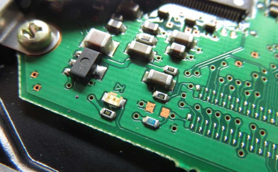
What are the Key Features of HDI PCBs?
- Microvias: A microvia is a plated blind structure with a maximum aspect ratio of 1:1 between its hole diameter and depth. Its depth should not exceed 0.25 mm from the land foil to the target plane or pad.
- Blind Vias: Blind vias are plated holes that run from the outer layer to any inner layer, but not through the entire PCB structure.
- Buried Vias: A buried via is a plated hole that runs through internal layers (between one or more) without exiting to the surface on either side, making it invisible from the outside.
- Via-in-Pad: Via-in-pads are plated holes positioned in the copper landing pad of a component. They are usually filled with non-conductive epoxy, capped, and then plated over.
- Sequential Buildup (SBU): This term refers to the process of building a multilayer PCB layer-by-layer using multiple copper sub-composites and thin insulating laminate materials.
What are the Advantages of HDI PCBs?
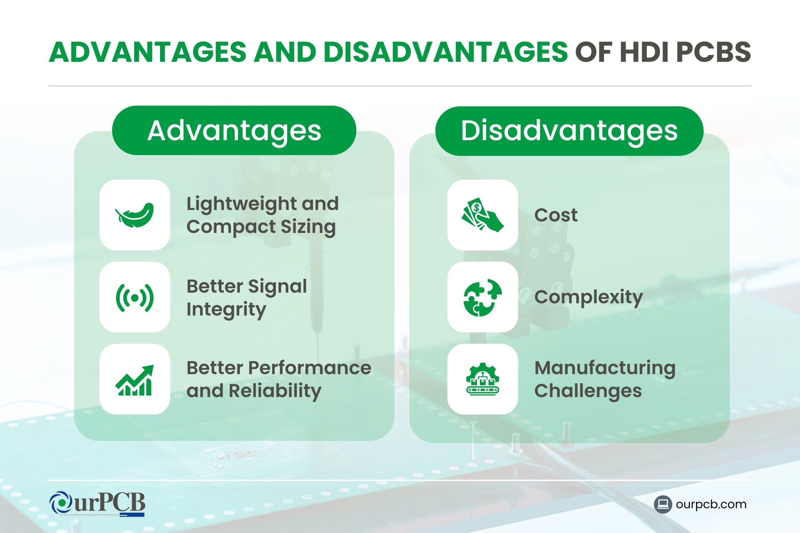
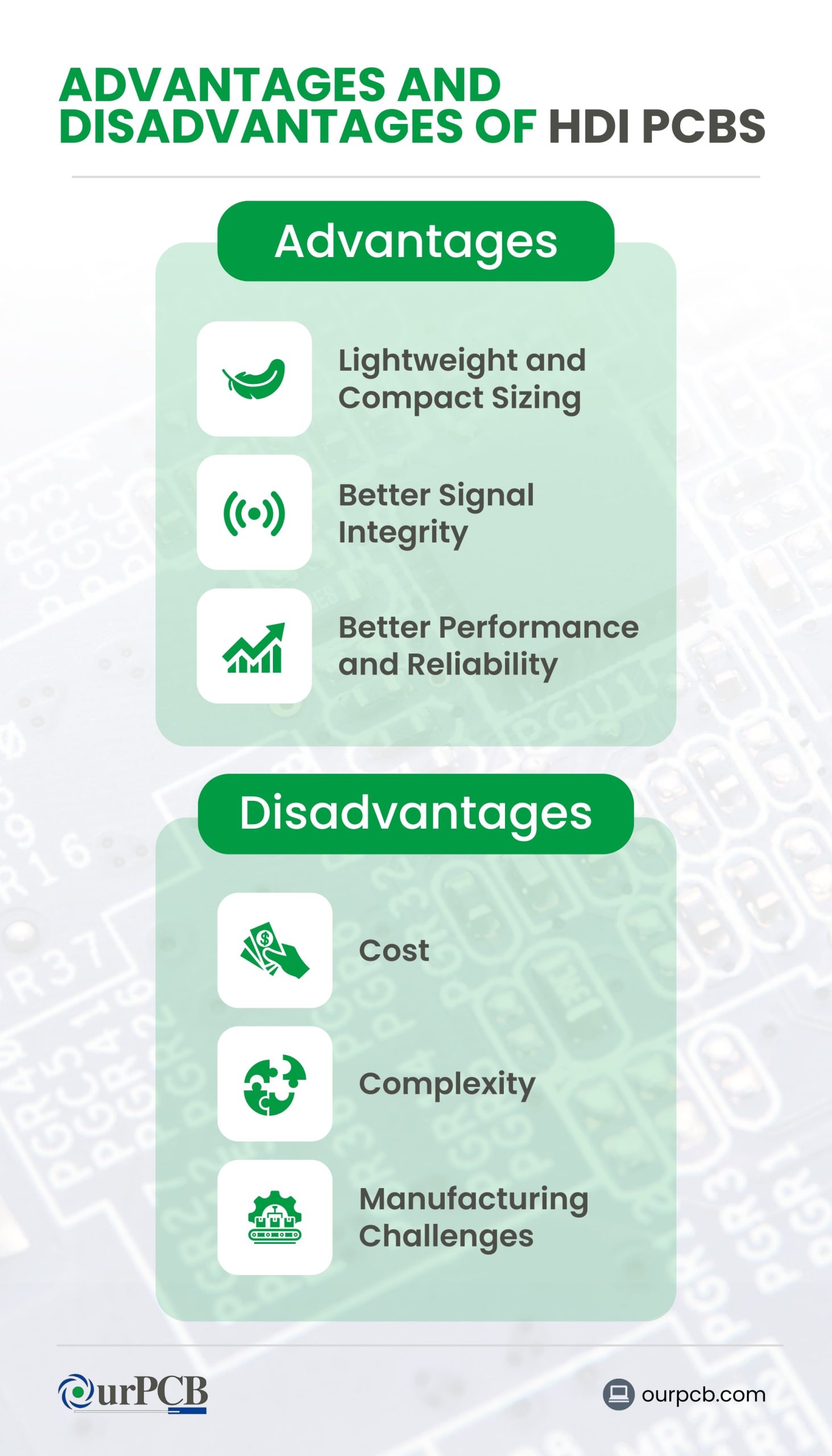
- Lightweight and Compact Sizing: The higher wiring density per unit area makes it possible to mount more components on a tiny board. This assembly creates a smaller circuit that is very useful for making devices like thin, powerful smartphones and tiny, multifunctional medical devices or wearables.
- Better Signal Integrity: Using more via structures, such as blind vias and via-in-pads, makes it possible to place components closer to each other, which reduces the signal transmission path. This design eliminates or reduces the occurrence of signal reflections, resulting in better signal quality through the circuit. Devices like wearables and phones will operate with zero glitches if they have improved signal integrity.
- Better Performance and Reliability: As active components like transistors form a tight-knit circuit on a small area, you can mount more of them to increase the board’s performance. The reduced signal reflections also enhance reliability.
By working with a trusted PCB manufacturer, companies can achieve optimal HDI PCB design and fabrication, maximizing performance while minimizing size constraints.
Special Offer: Get $100 off your order!
Email [email protected] to get started!
What are the Potential Disadvantages of HDI PCBs?
- Cost: HDI PCBs are costly to make because they require special, costly machines and more careful workmanship.
- Complexity: From as early as the design process, HDI PCBs need more meticulous planning. And during manufacturing, the small, multilayer board requires high attention to detail because it’s easy to make mistakes.
- Manufacturing Challenges: The manufacturing process takes time, especially as the layers increase. Additionally, mistakes like excessive copper etching can damage critical features on the board, and the process is generally not as environmentally friendly as regular PCB manufacturing, because it creates more waste.
HDI PCB Design Considerations
Materials Matter
When designing HDI PCBs, it is vital to note that these circuit boards require special dielectric materials that can handle the high heat levels generated by the components and traces. These materials should also handle the stresses associated with things like expansion due to heat.
Ideally, the core should be a low dielectric loss and low dielectric constant material to reduce heat management needs, maximize electrical efficiencies (in high-frequency applications), and prevent charge buildup.
The prepreg thickness is also an important factor to consider because this layer separates and isolates conductive tracks. It should be thick enough to prevent interference and thin enough to make the multilayer HDI PCB suitable for making tiny devices.
Software is Key
The CAD software used to design regular PCBs might not be sophisticated enough to handle HDI PCBs. Design software for HDI PCBs should be able to:
- Create the multilayer stack
- Give you precise control over the design rules and other constraints like the impedance
- Accommodate all the via types
- Provide powerful routing tools
Talk to the Manufacturer
Since HDI circuit boards are complex builds, it is important to liaise with the manufacturer from the product design process to ensure successful production. Sending ready designs to your fab house might require several revisions once the DFM, DFA, and DFT checks are complete. You can avoid all these delays by engaging your manufacturer during the design phase.
Layer Stackup is Crucial
HDI is synonymous with multilayer designs because the board must have multiple conductive layers to create a high wiring density in a small area. Therefore, getting the layer arrangement right is crucial to making the HDI PCB operate successfully.
Trace Design Matters
Besides having copper traces in multiple layers, these conductive tracks need to be thin so that many of them can fit in a small area. These tiny traces need careful designing to achieve impedance matching and avoid signal interference.
Vias are Everywhere
HDI circuit boards need multiple vias to interconnect the conductive layers. These vias don’t have the same design. When designing the PCB, you have to use the right via type for each section to achieve the required performance and functionality.
Component Placement is Key
The electronic parts should be close to each other to reduce the distance the signal travels, which reduces the chances of reflections along the path. Placing these components near each other also minimizes the routing space.
Signal Integrity is Everything
In high-speed, high-frequency HDI PCB designs, signal integrity is the most important aspect to consider. Some of the factors that contribute to better signal quality are impedance control, correct dielectric materials, reduced crosstalk, proper trace routing, and correct ground plane and layer stackup design. You should consider all these variables when designing high-speed, high-frequency PCBs.
What are the Main HDI Structures?
HDI structures are the layout options for these circuit boards, and they include the following.
Stacked Structure
1-n-1
1-n-1 stacked structures are the simplest HDI structures because they have one buildup of the high-density interconnected layers. They contain fine lines, superb mounting stability and reliability, microvia and registration technologies capable of 0.4 mm ball pitch, and can have copper-filled vias.
Building them requires one sequential lamination on either side of the core. Typical applications include MP3 players, memory cards, and GPS PCBs.
i-n-i (where i ≥ 2)
This stacked structure contains two or more buildups of HDI layers, where the microvias in the different layers can be stacked or staggered. Copper-filled vias are common in these designs to deliver high-level signal transmission performance.
The i number can reach high values, but the cost and complexity of the structure limit the buildup. This moderately complex structure can also include buried vias (i-bn-i) and is suitable for BGAs with smaller ball pitches and more I/O counts, such as those found in game consoles and portable video recording devices.
Any-Layer Structure
These are the most complex HDI structures because they allow conductors in any layer to be interconnected freely with laser-drilled, copper-filled microvias. This flexible structure provides a reliable interconnection for complex, large pin-count devices, such as the CPU and GPU chips used in mobile or handheld devices. These include small computing devices, smartphones, and ultra-mobile PCs.
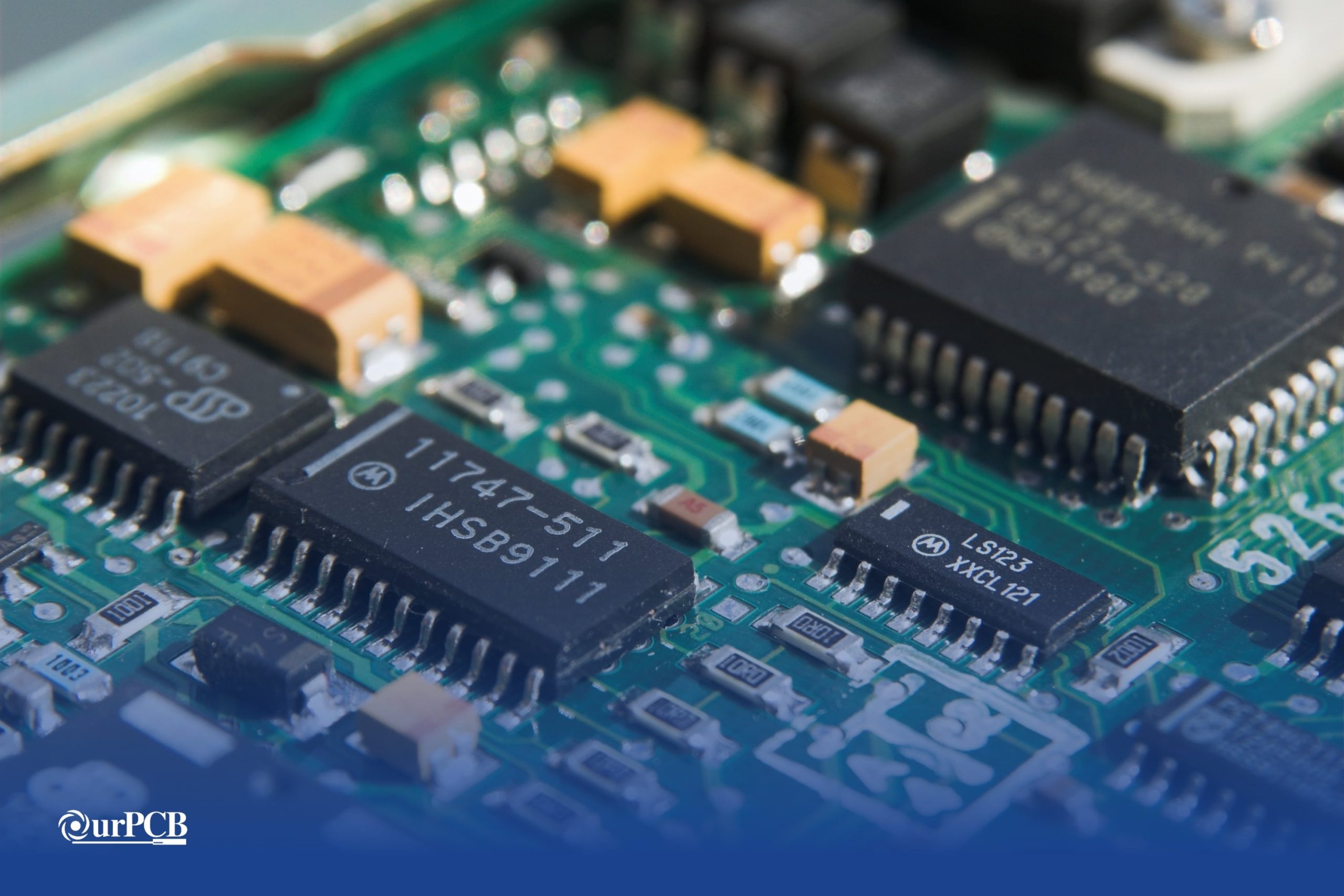
HDI PCB Manufacturing Process
Sequential lamination is the backbone of HDI PCB manufacturing, and it includes laser drilling to form the microvias. Combined, the HDI board manufacturing processes introduce manufacturing complexities that make these PCBs more expensive to make than regular PCBs. These processes include:
-
Sequential Lamination
Let’s use an example of a 2-4-2 stacked HDI PCB structure. The manufacturing process involves making and laminating the four inner layers in the regular way, which includes mechanical drilling and electroplating inner blind vias.
After that, layers 2 and 7 are manufactured and laser drilled to form the microvias. These layers are then laminated with the four inner layers (one on each side) using heat and pressure, then the microvias are electroplated. The two outer layers (1 and 8) are then manufactured, laser drilled, and finally laminated to the PCB to form the complete stack.
This process is known as sequential lamination. It gives good control over the board’s final thickness, forms strong bonds between the PCB layers, reduces the chances of warping, and prevents breaking or shifting during drilling.
-
Via Metallization and Filling
Fabricators usually use laser drilling to create microvias in HDI boards, after which they fill them using electrochemical plating, conductive epoxy, or conductive pastes containing silver or copper. This filling material should be conductive and sit flush with the land to form a flat solderable surface like a traditional land.
-
Materials Selection
The circuit boards can have core materials like FR4, Rogers, or metal, but the microvias should have conductive materials like copper or silver-filled pastes, conductive epoxy, or electrochemically filled plating. On the surface, ENIG is the most common finish because it forms a flat surface that is easy to solder.
Applications of HDI PCBs
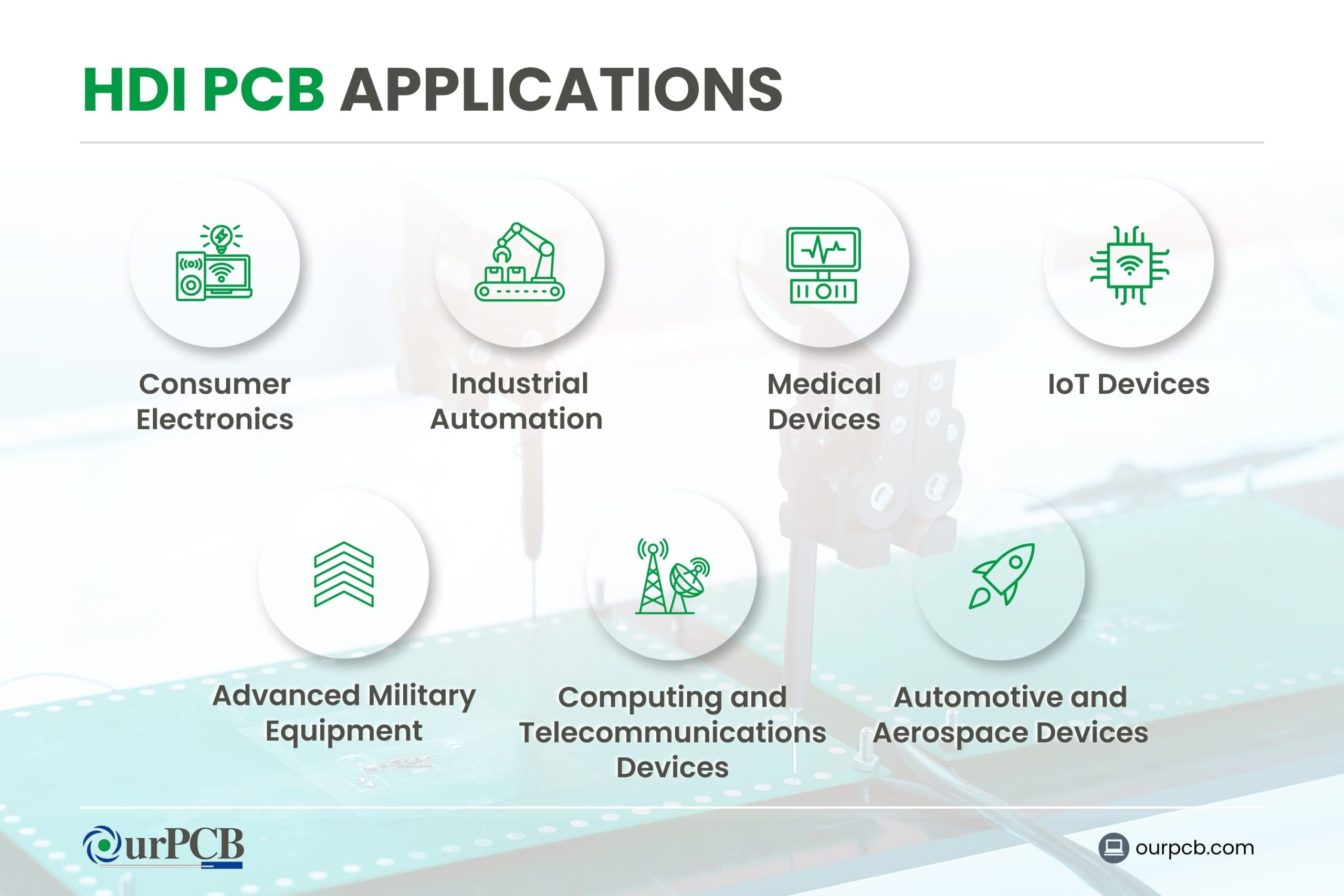
- Consumer electronics like touch-screen devices, smartphones, digital cameras, and laptops – HDI PCBs make these devices smaller.
- Automotive and aerospace devices, to make them provide more complex functionality in tiny packages.
- Medical devices like implants and diagnostic tools – HDI PCBs make them tinier, more accurate, cheaper, and perform better.
- Industrial automation and IoT devices are becoming more complex, and HDI PCBs make it possible to house these circuits in small packages.
- High-performance computing and telecommunications devices like 4G/5G networking equipment and servers handle high frequencies and need the signal integrity provided by HDI PCBs.
- Advanced military equipment also requires the performance, reliability, and signal integrity offered by HDI circuit boards.
High-Density Interconnect (HDI) PCB Technology FAQs
What’s the Difference Between HDI and a Traditional PCB?
Compared to a traditional PCB, an HDI board has a higher wiring density per unit area, smaller vias (microvias) that can be stacked, narrower traces, and more layers in the stack.
Can you Design an HDI PCB by Yourself?
Yes, but you’ll need specialized CAD software and HDI knowledge. As an experienced PCB designer, you should begin with simpler HDI circuit board projects, such as 1-n-1, to get up to speed. Also, consult your manufacturer during the design process.
How Reliable are HDI PCBs?
When designed and manufactured properly, HDI circuit boards are highly reliable because they experience less signal interference within the circuit. However, their complexity makes them challenging to design and manufacture, which can make them unreliable if not built well.
Back to top: High-Density Interconnect (HDI) PCB Technology
Special Offer: Get $100 off your order!
Email [email protected] to get started!