An electronic circuit designer must consider several aspects while designing circuit boards. Among them are ground-level separation, the board size, and how to place and design components. Also, PCB manufacturing assembly houses take extra precautions during fine pitch PCB design.It forms the basis of our discussion today. Hence, for a detailed elaboration of fine-pitch PCB assembly and what it entails, join us on a journey as we tackle everything about this delicate process.
Contents
- What is Fine Pitch PCB Assembly?
- Fine Pitch Components
- SMT Stencils for Fine-Pitch Assembly
- Fine Pitch Circuit Boards Design
- Fine Pitch PCB Layout Challenges
- 1. Select the right component sizes
- 2. Consider the component ratings
- 3. Choose the right board size
- 4. Place the components
- Other Considerations for fine pitch design board space-optimization
- Summary
What is Fine Pitch PCB Assembly?
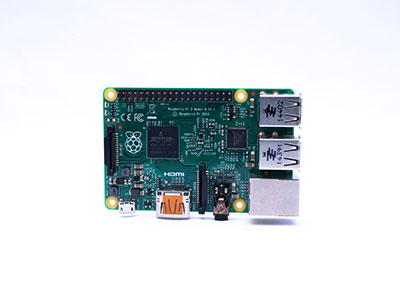
A fine pitch PCB
A fine pitch board is a PCB featuring a relatively high concentration of components per square inch. Also, due to the high density of components, it's common to find some referring to such PCBs as high-density PCBs.
In addition, the following characteristics define a fine pitch PCB:
- The screw terminal features 2.54mm pitch pins, ideal for alignment with the 0.1-inch perf boards.
- It also has screw terminal blocks measuring 2.54mm or 0.1-inch pitch. Thus, it is a handy alternative to the 0.1-inch female or male headers in most conventional PCBs.
- Lastly, it has a Veroboard pitch, essentially a 2.54mm hole in the copper track rows.
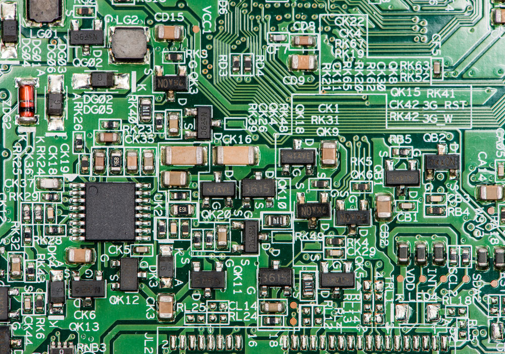
Fine Pitch Components
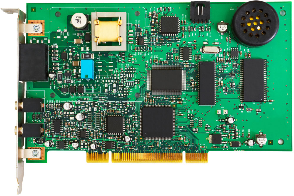
Several components on a PCB
You can have various components in fine pitch board assembly, including ICs, QFPs, BGAs, and SMDs. But, the rule of thumb is that the center-to-center distance separating the adjacent solder balls must be within 0.5mm.
Also, having a good solder connection is imperative. Lastly, most fine-pitch assembly surface mount devices vary from 0201, 0402, to 0603.
Special Offer: Get $100 off your order!
Email [email protected] to get started!
SMT Stencils for Fine-Pitch Assembly
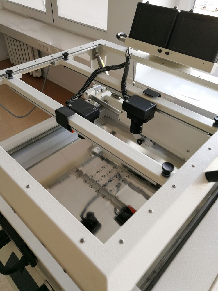
Surface mount technology solder paste stencil with perforated holes
Fine pitch PCB assembly requires laser-cutting stainless stencils featuring apertures. Also, given the small size of fine-pitch SMDs, the fine-pitch PCB pads are relatively small. Hence, solder paste printing on such a pitch board is an arduous undertaking.
Also, factors such as stress concentration render solder paste insufficient for use in QFPs and fine pitch ICs.
Thus, these shortcomings prompt Fine-pitch board vendors to create SMT stencils for PCBs. Also, their apertures are of different sizes and shapes from the PCB pads for improved efficiency.
Fine Pitch Circuit Boards Design
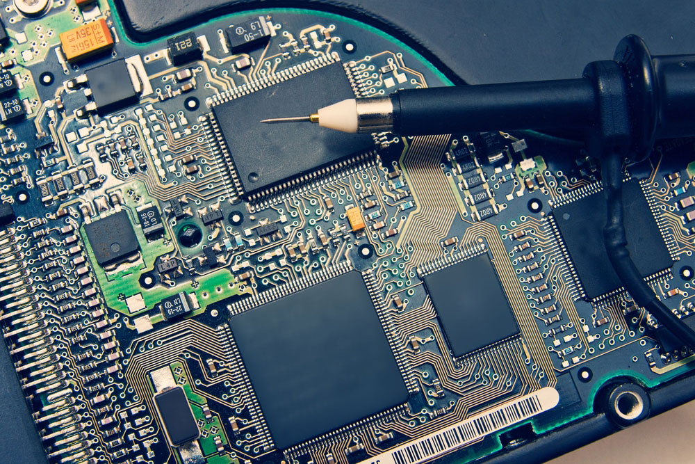
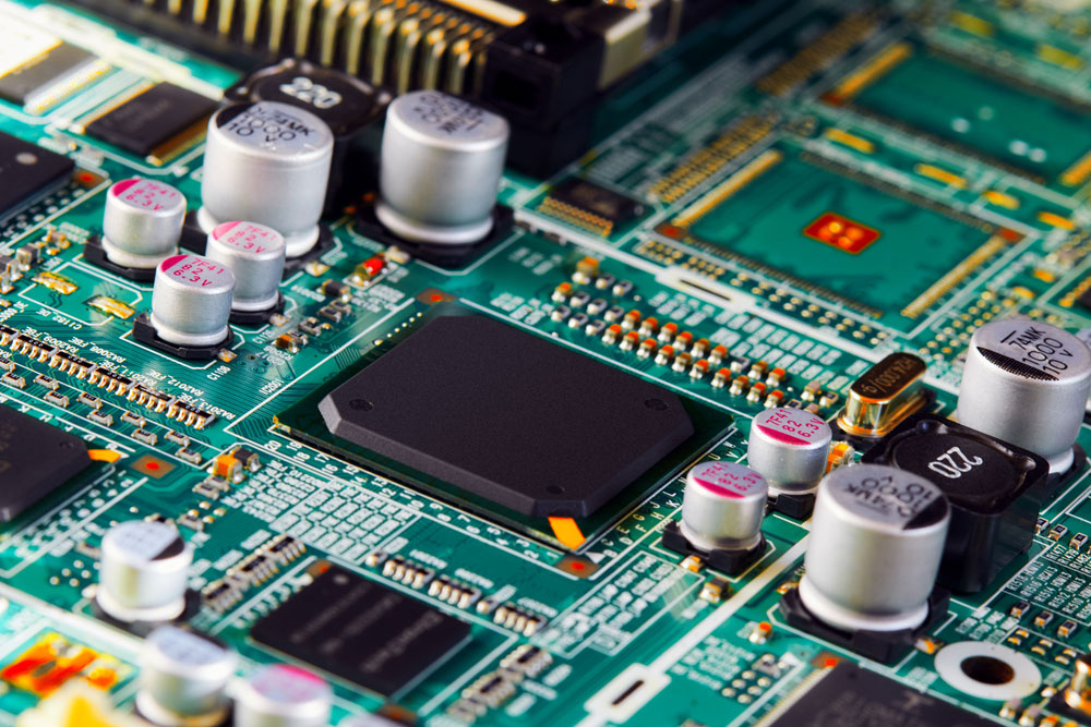
An oscilloscope probe on a high-density PCB
Ideally, a large concentration of board connectors featuring an extensive network of fine-pitch components will complicate the fabrication process. Also, designing a minute-millimeter pitch board requires precise pick and place machines.
Besides, the design process is further complex if the board assembly vendor applies grid-array-based components or leadless types. This fine array of board stacking would necessitate X-ray inspection for exact precision and design accuracy.
Therefore, during the board connector solutions and design, the board designer and the board vendor should closely cooperate.
Fine Pitch PCB Layout Challenges
As highlighted above, achieving a fine pitch board stacking interconnect is challenging. Thus, for a successful connection of the fine-pitch parts, board houses must religiously follow the following steps:
1. Select the right component sizes
PCB with various electronic parts
Before embarking on the PCB layout for the fine pitchs board products, choosing suitable component sizes is imperative. Ideally, board space savings is crucial as most boards are not too large.
Moreover, board connection and assembly of finer pitch components can be a cost-intensive task. And this is especially true when additional operations such as X-Ray inspection are a prerequisite.
Nonetheless, board space optimization may prove hard when the priority is bringing the board systems manufacturing costs down. In such a case, manufacturers will compromise fine pitchs basic design parameters and go for bulky components.
2. Consider the component ratings
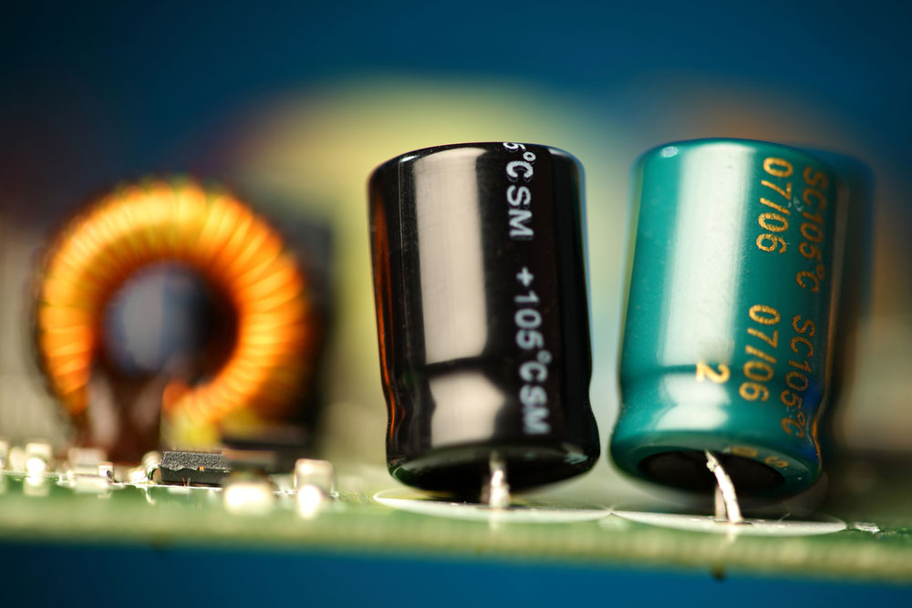
PCB parts and power supply ratings
You need to work within a reasonable power rating margin when choosing the individual components for the high-density pitch.
For instance, a 50V capacitor is not ideal for a 10V rail. Ideally, the best option should be within a 20-30% capacitor voltage rating. Hence, going for a 10V will still be too close to the rail rating. Instead, a 16V or so capacitor would be the best.
3. Choose the right board size
Determining the right size is critical as it defines its feasibility in fitting components.
First, manufacturers will identify the smallest possible size by placing board connectors and buky components on the board. Also, it's essential to consider the sensitive traces on the board that require separation from the rest of the components.
In most cases, picking preset board sizes and shapes helps in cost saving. Also, in addition to the traces, you must make crucial considerations for the board's clearances.
4. Place the components
After picking the right board size, it's time to place the components on the board. Begin with high-power and high-speed components. Also, this process necessitates considerations for the available planes, vias, and traces.
Other Considerations for fine pitch design board space-optimization
High tech PCB
-
Creating Via-in-pads
Most PCB assembly houses don't consider this design as necessary. Nonetheless, creating vias on the components pads saves routing space. The process is tricky, though, as it may compromise the quality of the component's solder connection.
-
Creating Fiducial marks
These imaging system's guide markers are handy in guiding the pick and place machine on the PCB's edges.
-
Leaving out Decoupling capacitors
When included, many assembly houses place them close to the sensitive pins. Still, leaving them out is a viable option, though this can introduce noise to analog/digital signals.
-
Adding Tooling holes
Tooling holes are handy in PCB alignment, especially for the effective operation of solder stencils and the pick and place machines.
-
Providing Testing points
They facilitate the testing of each part, which can be a complicated exercise considering the density of the fine pitchs assembly array.
Summary
In a nutshell, fine pitchs design is an intricate procedure necessary for many board applications' success. Above is an explicit elaboration of how manufacturers tackle each step to generate micro millimeter pitch boards. That's all for today but communicate with us for further questions and queries.
Special Offer: Get $100 off your order!
Email [email protected] to get started!