The surface-mount packages for integrated circuits mounted on PCBs come in different types. However, the most popular ones are QFP vs QFN. The two have several varieties, but their issues and assembly processes are similar.If you have to mount such devices to your circuit board, it is vital to understand what they are and how to assemble them. We have covered these topics in detail below, so take a look!
Contents
- QFP vs. QFN: QFN Package
- QFN Variations
- Plastic-Molded
- The Air-Cavity QFN
- Wettable Flanks QFN
- The Punch-Type QFN
- The Sawn Type QFN
- Flip Chip QFN
- Wire Bond QFN
- Advantages of QFN Packages
- QFN Issues
- Manufacturing Issues
- Soldering Issues
- Compatibility Issues
- QFN Footprint Design
- QFN Assembly
- Solder-Paste Printing
- Component Placement
- Pre-Reflow Inspection
- Reflow Soldering
- Post Reflow Inspection
- Rework an Assembled Component
- QFN Soldering
- QFP vs. QFN: QFP Packages
- QFP Package Variations
- Bumper Quad Flat Pack (BQFP)
- Bumper Quad Flat Pack Having Heat Spreaders
- Ceramic Quad Flat Packages
- Fine Pitched Quad Flat Packages
- Heat-Sinked Quad Flat Pack
- Low Profile Quad Flat Packages
- Metric Quad Flat Packages
- Plastic Quad Flat Package
- Thin Quad Flat Package
- Issues to Consider When Dealing With QFPs
- QFP Damage
- Density Track on the Printed Circuit Board
- Advantages and Disadvantages of QFP Packages
- Advantages
- Disadvantages
- QFP Chip PCB Assembly
- Stencil Printing (Solder Paste)
- Component Placement
- Reflow Soldering
- QFP vs. QFN: Difference Between QFP and QFN
- Lead
- Assembly
- Pin Count
- Summary
QFP vs. QFN: QFN Package
QFN is an acronym for Quad Flat No-lead package. Its function is to link the IC's silicon die to the circuit board. A copper-lead frame with a matt tin coating surrounds the die, and bond wires connect the two parts. However, some manufacturers use flip-chip technology to connect the two sections because it offers better electrical performance.
This silicon die sits on an epoxy material, which attaches to the exposed metalized pads. These pads provide electrical connections and ground paths to the PCB. QFN packages are usually tiny and provide moderate heat dissipation to the PCB.
QFN Variations
QFN packages are available in the following types.
Plastic-Molded
As one of the most affordable QFN packages, this variation doesn’t have a lid and consists of only two sections.
- Plastic composite compound
- Copper-lead frame
But this type's applications only lie between 2-3 GHz.
The Air-Cavity QFN
These QFNs contain an air enclosure in the package and have three sections.
- Copper-lead frame
- Plastic/ceramic Lead
- A plastic-molded body that you open with/without a seal
The air-cavity type is more expensive than other QFNs due to its construction. However, it has a wider application range that lies between 20-25 GHz.
Wettable Flanks QFN
These flanks have an elevated base to show the solder wetting. Therefore, you can inspect the pads to check if they sit correctly on the circuit board.
The Punch-Type QFN
Such QFNs have a single-mold cavity setup containing the molded package, with a punch tool splitting this cavity, hence the name. But the QFN is also available as a single package molded up via this method.
The Sawn Type QFN
This package utilizes the mold array process for molding. The process entails cutting one large box into tiny chunks, then sorting them.
Flip Chip QFN
Flip-chip QFNs use flip-chip technology to connect the copper-lead frame to the silicon die. This technology creates a shorter electrical connection between the two, making it ideal for electrical applications.
Wire Bond QFN
As the name suggests, the QFN uses wires to connect the chip's terminal to external components. Wire bonding directly connects to an integrated circuit, PCB track, or semiconductor.
Advantages of QFN Packages
- Lightweight and easy to handle
- Thin profile (less than 1mm) with a tiny footprint
- Short bond wires for connecting the die to the frame
- Low lead inductance
- No lead coplanarity problem
- Incredible heat dissipation
- Requires regular surface-mount equipment for circuit board assembly
- Affordable
QFN Issues
QFN packages are pretty good, but they have a few issues.
Manufacturing Issues
QFN packages perform exceptionally well in low-mix, high-volume products. However, they encounter challenges in minimizing fault rates during placement and reflowing in high-mix, low-volume scenarios. This problem primarily affects the board and stencil design.
Therefore, you should use accurate stencil designs and thicknesses and strictly follow manufacturer guidelines. Check the aperture-pad ratio, soldering thickness, etc. On the other hand, the bond pad design should lie at a 0.2-0.3 range from the package base.
Soldering Issues
Because QFN packages feature slim pad-to-pad pitches, they create a potential solder bridging problem. Also, you might encounter issues desoldering the packages because they don't have Lead.
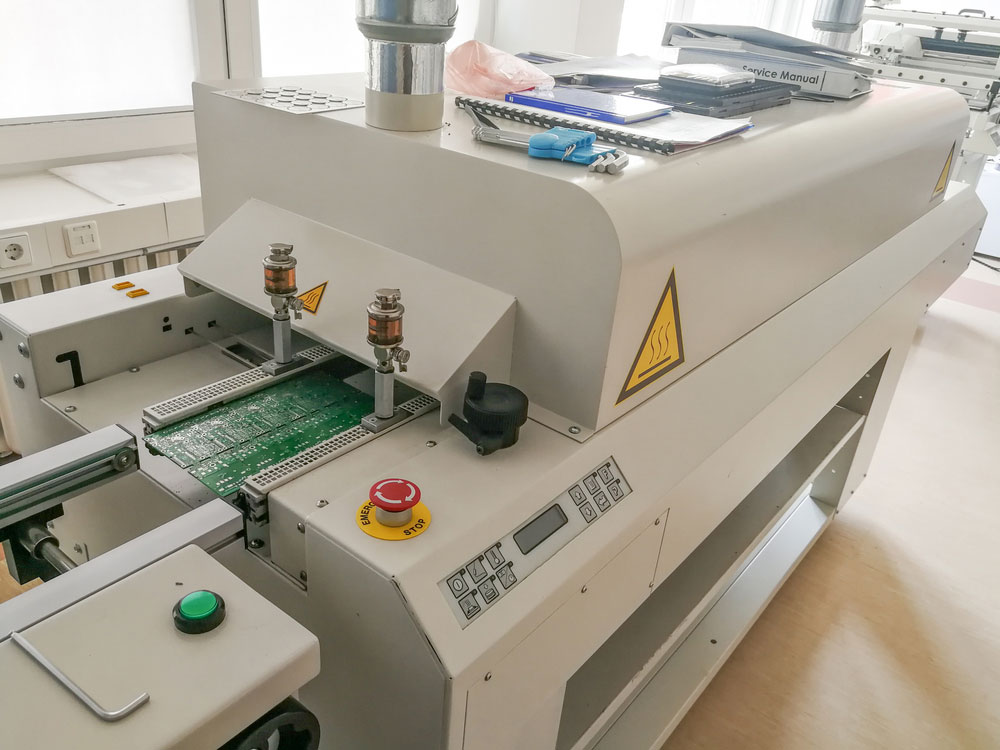
A PCB heading into a reflow oven after assembly
Compatibility Issues
The lack of Lead can change the dimensions of the package or board they sit on. Therefore, they become weaker after experiencing nominal OEM or CM practices.
Besides that, they might experience board flexure due to the high stress experienced after in-circuit testing, board attachment, etc. This issue occurs because the packages lack long, flexible copper leads.
QFN Footprint Design
Always refer to the QFN datasheet when designing its footprint because it shows the outline's drawing. Also, observe the following factors.
- The EP/ ground pad should have enough vias for heat dissipation
- Pin 1/ orientation marking
- Ensure the solder bridge is 4mil or higher
- Check the solder paste and solder mask layers (observe openings recommendation by the manufacturer)
QFN Assembly
Assembling a QFN component on a circuit board involves the following steps.
Solder-Paste Printing
Solder paste printing entails spreading the solder paste uniformly on the PCB, a necessary step before component placement.
Component Placement
Next, embed the QFN integrated circuit on the PCB as per the board layout design. Use a precise pick-and-place tool for maximum accuracy due to the high interconnection density.
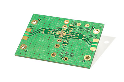
The footprint of a QFN footprint on a PCB
Pre-Reflow Inspection
This step is crucial because you must ensure the PCB and placed components are ready for soldering. Also, check for surface board contaminants that might affect the soldering process.
Reflow Soldering
If everything looks good, place the PCB in the reflow oven.
Post Reflow Inspection
Check the soldering quality. Although not expected, there might be some issues.
Rework an Assembled Component
Should a QFN soldering defect, you must rework that component by plucking and placing it again. Do this procedure using the following steps.
- Do a pre-bake procedure to avoid moisture-related failures
- If you must desolder, keep your component's temperature profile in mind
- Remove the part mechanically from the PCB after desoldering
- Clean the circuit board pads and remove the residue
- Follow the 5-step assembly procedure above to attach the component back to the PCB
Special Offer: Get $100 off your order!
Email [email protected] to get started!
QFN Soldering
Soldering is the fourth step in the QFN assembly process. When the PCB enters the reflow oven, some parts heat faster than others. This uneven heating occurs due to temperature variation in the reflow oven.
Parts that heat faster become lighter, while those that heat up slower are large copper sections or heavy components,
Therefore, you can monitor the QFN package's surface temperature during the soldering process. The goal is to ensure the package's peak body temperature does not surpass preset values.
QFP vs. QFN: QFP Packages
QFP is an acronym for Quad Flat Package. Like QFN, QFP is a surface-mount IC package, but this one features "gull-wing" leads/pins extending from all four edges.
Such packages are standard in large-scale and very large-scale integrated circuits. With the pin count being over 100, this integrated circuit package is very efficient and reliable. Therefore, it is ideal for packaging central processing units.
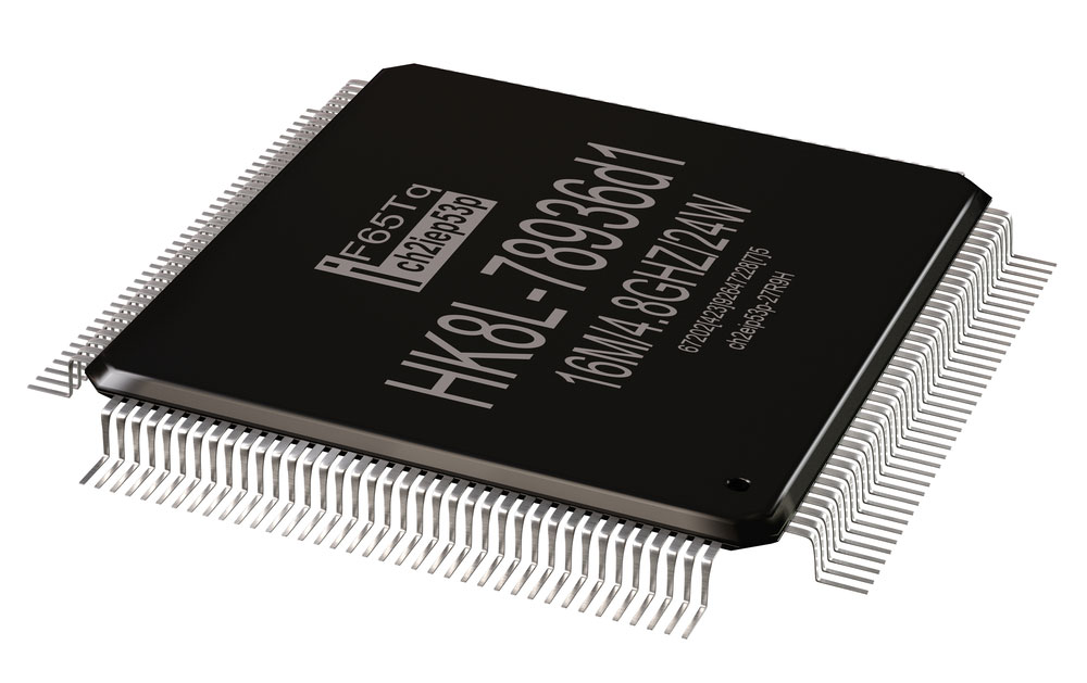
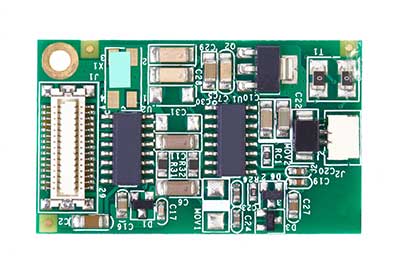
An IC with a QFP package
Additionally, QFPs have tiny parasitic parameters, making them ideal for high-frequency applications.
This package can be in a square or rectangular shape. The former has an equal pin count on all sides, while the latter has a different pin count on each side.
QFP Package Variations
Besides the shape, QFP packages have the following variations.
Bumper Quad Flat Pack (BQFP)
BWFP packages feature shield extensions on all corners to protect the leads from mechanical damage pre-soldering. These lead pins can get easily bent or damaged, while their fine pitch makes them almost impossible to repair if turned.
Bumper Quad Flat Pack Having Heat Spreaders
This variant is similar to BQFP but adds heat spreaders to enhance efficiency by allowing quick dissipation at higher power levels.
Ceramic Quad Flat Packages
This package utilizes ceramic as the base material, which improves quality and efficiency.
Fine Pitched Quad Flat Packages
As the name suggests, these QFP packages feature a fine pitch.
Heat-Sinked Quad Flat Pack
Integrated circuits with high pin counts can dissipate high heat levels. This heat needs efficient dissipation for optimal IC performance. You can create a heat sink for such packages by replacing some pins (usually on the opposing side's central part) with thicker ones. Next, solder these pins to a broader pad with a wide copper area on the PCB. This setup should dissipate heat much faster.
Low Profile Quad Flat Packages
These packages are unique due to their slim body thickness (1.4mm). They have the following specs based on QFP and MQFP metrics.
- 2mm lead-frame footprint
- 32 - 256 lead count range
- Varying body size from 5x5mm to 28x28mm
- Four varying lead pitches (0.3, 0.4, 0.5, and 0.65mm)
Metric Quad Flat Packages
Regular QFPs use imperial measurements to define their sizes, but this variant uses metric measurements.
Plastic Quad Flat Package
These QFP packages have a plastic build quality.
Thin Quad Flat Package
TQFPs are also plastic-built but have a low profile design with a 1mm height. However, their lead frame footprint is standard (2mm)
Issues to Consider When Dealing With QFPs
QFP Damage
Quad Flat Package pins are tiny and also have small spacings between them. This design renders them vulnerable to permanent or difficult-to-fix damages. Therefore, always store them carefully and pack them in special waffles during transportation.
Density Track on the Printed Circuit Board
Since a QFP can have several hundred pins, you must consider this during your PCB design process. Otherwise, you might have track density issues.
Advantages and Disadvantages of QFP Packages
Advantages
- Utilizes mature technology
- Can utilize sockets
- Square QFP packages can accommodate a higher pin density than the rectangular type
.
Disadvantages
- 500MHz I/O limit
- Inadequate complex input/output chips
- Square packages are more fragile due to their high pin density.
QFP Chip PCB Assembly
Assembling a QFP chip on a PCB requires the following steps.
Stencil Printing (Solder Paste)
This step involves applying solder paste via a stencil. Excessive solder paste can cause bridging, while inadequate application reduces spreading. Therefore, consider the stencil's thickness and aperture for accurate sizing.
Also, you should use a suitable solder paste, such as type 4. Lead-free solder pastes usually contain a tin-silver-copper alloy, and these particles must fit in the stencil apertures when printing.
Component Placement
Next is component placement. QFP components self-align due to the liquid solder's surface tension, resulting in reliable solder joints. But you still have to position the component precisely, and you can achieve this using a P&P machine.
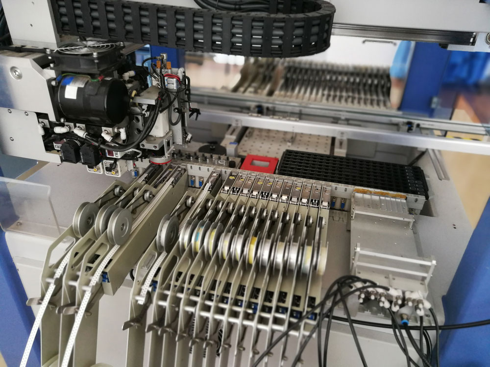
A pick-and-place machine
Reflow Soldering
It is best to use a force convection oven for reflow soldering because it does the process in a nitrogen-filled atmosphere. But this is not necessary. The crucial thing is to consider the manufacturer guidelines.
QFP vs. QFN: Difference Between QFP and QFN
QFP and QFN packages differ in the following three areas.
Lead
QFP packages contain leads that extend outwards on all sides in a gull-wing (or L) shape. However, QFN packages have no pin leads, hence the name (no-lead package). Instead, they contain metalized contacts on the underside.
Assembly
QFPs have an excellent footing due to the leads and self-align during the assembly process. However, QFNs have an average base footing during assembly. Therefore, they require careful placement plus keen inspection before and after reflow soldering.
Pin Count
QFP packages have several pins ranging from as little as 32 (eight on each side) to as many as 280 (70 on each side) or higher. However, QFNs usually have a few pins (eight plus a thermal pad).
Summary
In conclusion, QFN and QFP are vital mounting options for integrated circuits. However, they have critical differences that require slightly different mounting procedures. We hope the article has been insightful and if you have any questions or comments, leave a message, and we'll be in touch.
Special Offer: Get $100 off your order!
Email [email protected] to get started!