There's nothing a designer or electrician hates more than an ENIG black pad.
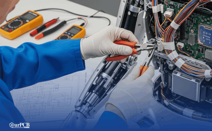
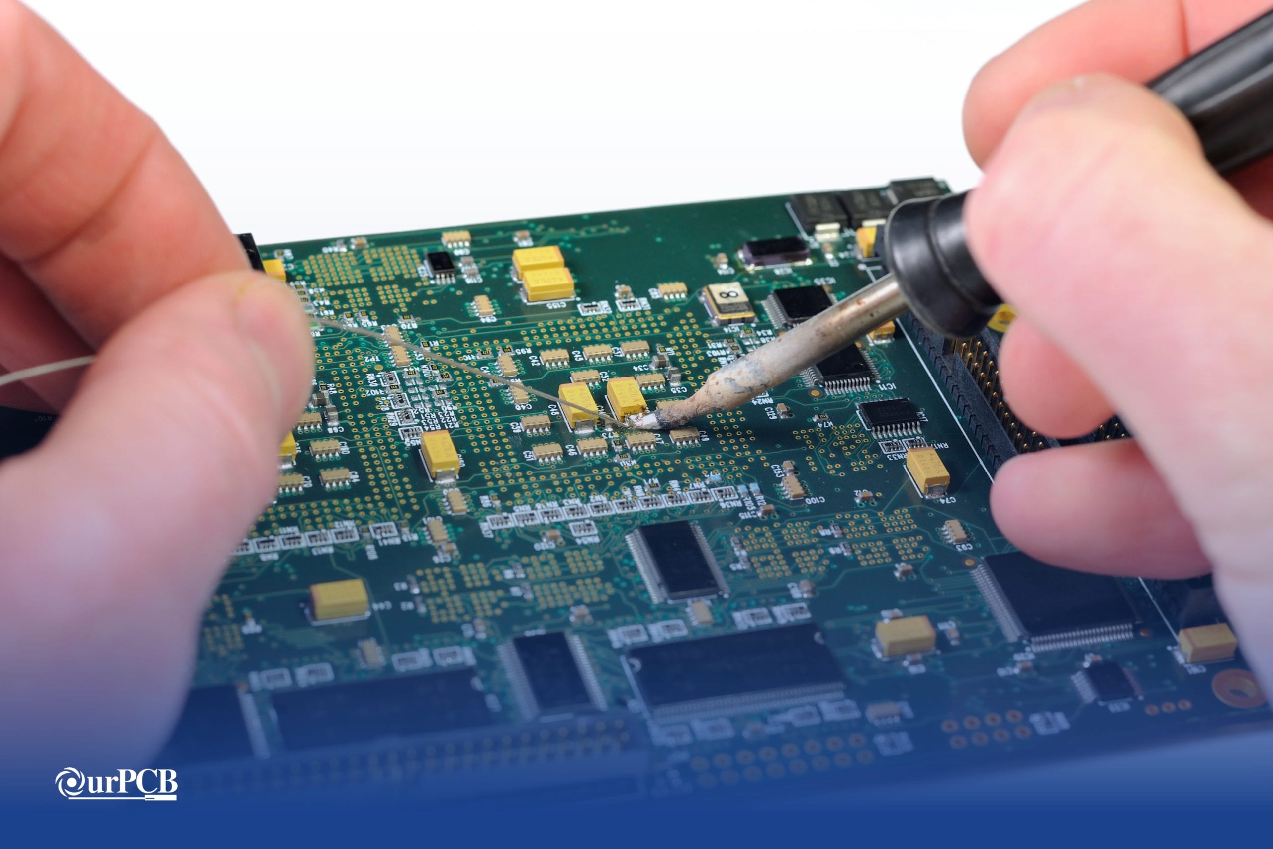
When it comes to printed circuit board (PCB) manufacturing, your surface finish plays a really important role in the quality and reliability of your electronic components.
Electroless nickel immersion gold (ENIG) is a very popular finish because it has great solderability and protection against oxidation. However, black pad is a common issue.
In this guide, we'll look into black pad ENIG, what causes it, how to prevent it, and how to fix it. Let's dive in!
Contents
- Key Takeaways
- What Are ENIG Black Pads?
- What Causes Black Pads?
- The Consequences of Black Pads
- How Do I Prevent Black Pad?
- How Do I Fix ENIG Black Pads?
- Rework and Replate
- Local Repair
- Alternative Joining Methods
- Adjust Soldering Parameters
- Try Additional Testing
- OurPCB: Expert PCB Manufacturing Services
- What Is the Meaning of ENIG Black Pads? | FAQs
- Is black pad still an issue for ENIG?
- What is the primary advantage of ENIG over other surface finishes?
Key Takeaways
- ENIG black pads are a critical defect that can weaken solder joints and compromise the reliability of electronic components.
- Black pads can lead to field failures, increased manufacturing costs, and even damage to a company's reputation due to product recalls or warranty claims.
- ENIG black pads are caused by corrosion of the nickel layer in PCBs.
- Key factors contributing to black pad formation include incorrect phosphorus content in the nickel layer, acidic immersion gold baths, poor process control, contamination, and insufficient nickel thickness.
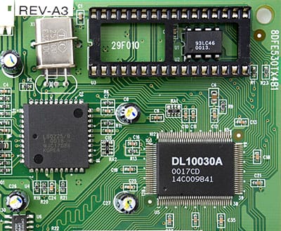
What Are ENIG Black Pads?
ENIG black pads, sometimes called “black nickel syndrome”, are a defect that can take place during the ENIG surface finish process on PCBs. This defect looks like dark or black areas on the nickel surface layer beneath the gold plating. You can usually see it after the gold layer has been removed during soldering or testing.
The ENIG finish is made up of two layers: an electroless nickel layer applied directly onto the copper surface of the PCB, followed by a thin immersion gold layer. Typically, this is a great combination for solderability and oxidation protection. However, when a black pad occurs, it damages the integrity of the nickel layer. This can lead to weak or unreliable solder pad joints.
Black pads are not always immediately obvious. Sometimes, you can only see them during the assembly process or after the product has been used for quite a while.
What Causes Black Pads?
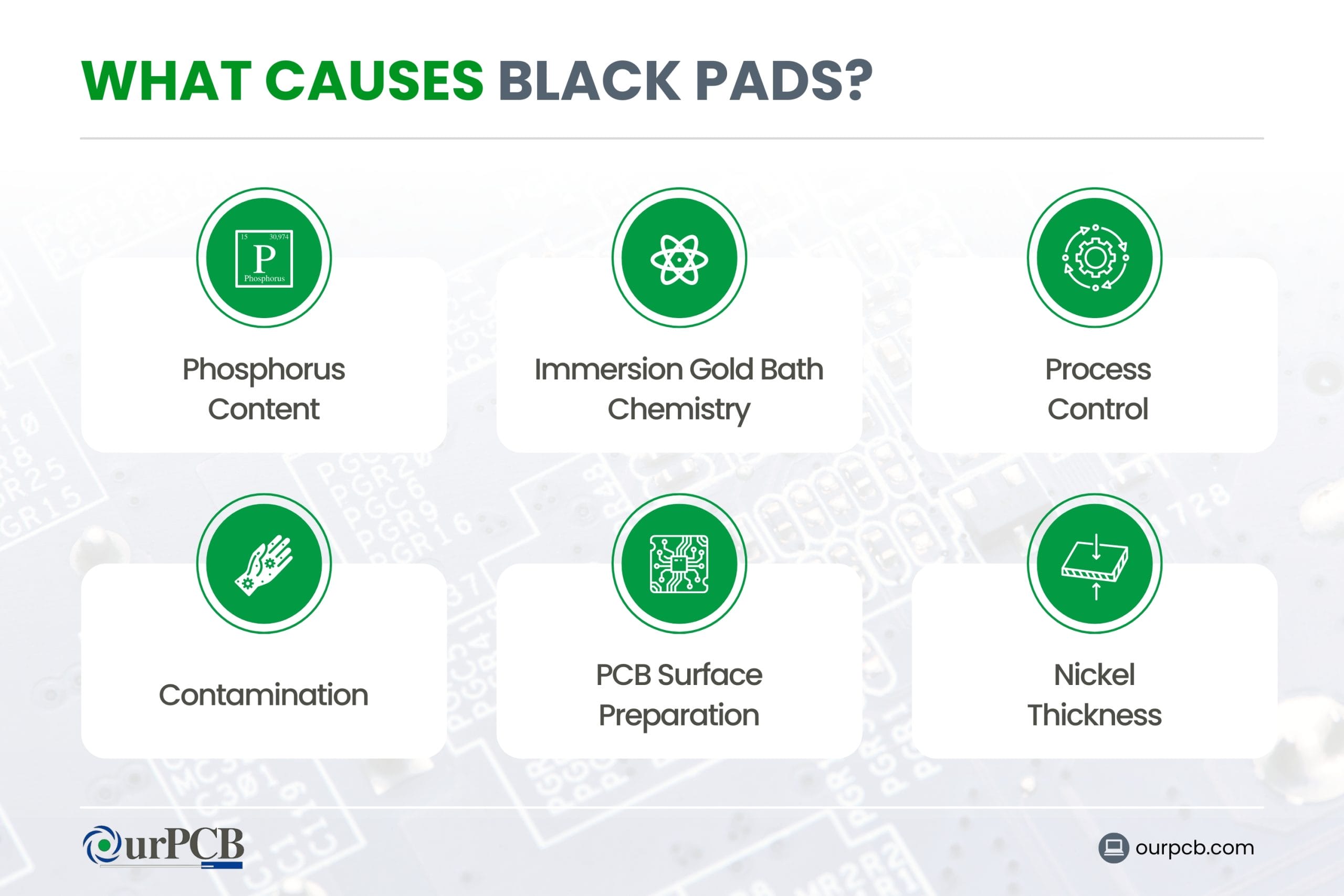
Black pads in your PCB design are usually caused by too much corrosion in the electroless nickel layer. Here are a few specific factors that can cause this corrosion:
- Phosphorus Content: The quality of the nickel layer is incredibly important. If your nickel layer has low phosphorus content, it would likely be corroded during the gold immersion process.
- Immersion Gold Bath Chemistry: An overly acidic gold bath can significantly speed up the corrosion of the nickel layer. The displacement reaction between nickel and gold can become too aggressive, which leads to uneven deposition and black pad formation.
- Process Control: If you lack control of the ENIG process parameters, such as temperature and pH, this can contribute to black pad problems.
- Contamination: If there are contaminants in the electroless nickel or immersion gold baths, it can cause trouble with proper deposition and lead to corrosion.
- PCB Surface Preparation: If you don't clean or prepare the copper surface properly before the ENIG process, it can result in poor adhesion and increase the risk of the formation of black pads.
- Nickel Thickness: A very thin nickel layer might not provide enough protection against corrosion during the gold immersion step.
Special Offer: Get $100 off your order!
Email sales@ourpcb.net to get started!
The Consequences of Black Pads
If you get black pads with ENIG finishes, you might be facing some pretty severe consequences. Here are a few black pad issues with ENIG finishes:
- Weak Solder Joints: Black pads can lead to poor solderability, which causes weak or unreliable solder connections. If you don't have reliable solder joints, it can even result in intermittent electrical failures or the complete disconnection of components.
- Reduced Product Lifespan: Devices with black pad issues might experience an early failure, leading to shortened product lifespans and increased warranty claims.
- Increased Manufacturing Costs: Looking for and fixing black pad problems usually requires extra inspection and rework. This can seriously drive up production costs.
- Reputation Damage: For PCB manufacturers and OEMs, recurring black pad issues can damage their reputation and lead to loss of customer trust.
- Field Failures: Black pad-related issues might not be obvious immediately, possibly causing devices to fail after they've been deployed in the field. This can lead to expensive recalls or repairs.
- Compromised Reliability: Even if initial solder joints look okay, the root cause of corrosion can continue to progress, potentially causing more failures over time.
- Design Limitations: The risk of black pads might force designers to avoid ENIG finishes for certain applications. This can limit design options.
Many of these problems are quite serious. Luckily, the prevention of black pad issues is completely possible and easy to achieve!
How Do I Prevent Black Pad?
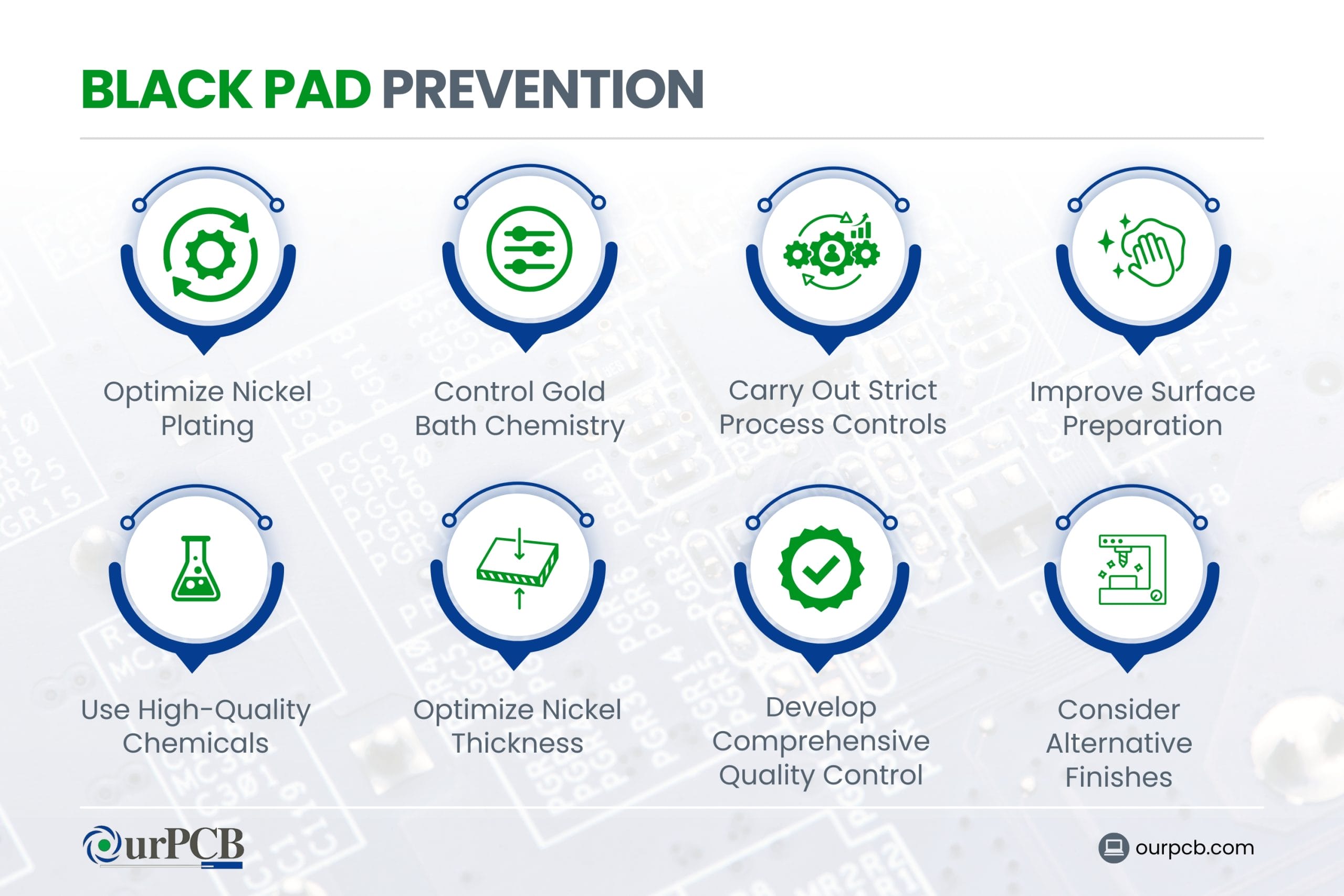
Preventing ENIG black pads takes a bit of extra work and addresses various parts of the PCB manufacturing process. Here are some helpful strategies to lower the risk of black pad formation:
- Optimize Nickel Plating: Make sure the electroless nickel plating process produces a high-quality nickel layer with the right amount of phosphorus content. This usually involves maintaining a mid to high phosphorus content (7–11%) in the nickel deposit.
- Control Gold Bath Chemistry: Carefully monitor and control the pH, temperature, and composition of the immersion gold bath. If you use less acidic gold baths, it can help reduce aggressive corrosion of the nickel layer.
- Carry Out Strict Process Controls: Create and maintain tight control over all ENIG process parameters, including immersion times, bath temperatures, and chemical concentrations.
- Improve Surface Preparation: Make sure you clean and prepare the copper surface thoroughly before the ENIG process. This can bring about good adhesion and consistency in deposition.
- Use High-Quality Chemicals: Find high-purity chemicals for the ENIG process and carry out regular bath maintenance to prevent contamination.
- Optimize Nickel Thickness: Make sure that the nickel layer is thick enough to support the gold immersion process without too much corrosion.
- Develop Comprehensive Quality Control: Regularly inspect and test ENIG-finished PCBs using methods such as X-ray fluorescence (XRF). This is to verify proper nickel and gold thicknesses.
- Consider Alternative Finishes: For critical applications, check out alternative finishes for the surface of the pad that might be less prone to black pad issues.
By trying out these preventive measures, PCB manufacturers can reduce the risk of black pad formation during PCB assembly and ensure more reliable ENIG finishes. If you've already experienced the black pad phenomenon, don't stress — there are still ways you can fix it!
How Do I Fix ENIG Black Pads?
Prevention is always better than having to fix black pads. Luckily, it's still possible to fix them after they've occurred, even though it can be challenging. Here are a few tips to fix ENIG black pads:
Rework and Replate
In some cases, it might be possible to remove the affected ENIG finish and replate the PCB. This process involves carefully stripping the gold and nickel layers and then reapplying the ENIG finish using the most effective parameters.
Local Repair
For isolated black pad problems, localized repair techniques can be used. This can involve safely removing the affected area and applying a new surface finish, such as selective gold plating.
Alternative Joining Methods
In situations where black pads are discovered during assembly, alternative joining methods like conductive epoxy or mechanical fastening can work.
Adjust Soldering Parameters
Changing soldering qualities, such as increasing temperature or dwell time, can help improve solder joint reliability on the boards with issues.
Try Additional Testing
If these methods don't work, going forward, you should improve testing protocols. This can help you find potential black pad issues before they lead to field failures. Testing might include more detailed solderability testing and cross-sectional analysis. A root cause analysis could also find the cause of the formation of black nickel can help prevent it in the future.
While getting rid of a potential ENIG black pad is a challenging job in the PCB industry, it's definitely worth it. However, prevention is still the best approach when it comes to black pad syndrome!
OurPCB: Expert PCB Manufacturing Services
Black pads are common issues in electronics, caused by nickel corrosion on PCBs. If you don't sort the issue out as soon as possible, it can lead to weak solder joints and electrical shorts.
Paying attention to the PCB manufacturing process is essential to avoid these problems. OurPCB offers expert PCB manufacturing services that ensure high-quality surface finishes, helping to reduce the risk of black pad formation and improve the reliability of your electronic products. Reach out for a quote!
What Is the Meaning of ENIG Black Pads? | FAQs
Is black pad still an issue for ENIG?
Yes, black pad is still an issue for ENIG. There have been huge improvements in ENIG processes to reduce the risk of black pads, but it's still a potential issue.
What is the primary advantage of ENIG over other surface finishes?
One of the biggest advantages of ENIG surface treatment over other finishes is that it has a great combination of flat surface planarity, long shelf life, and superior solderability.
Special Offer: Get $100 off your order!
Email sales@ourpcb.net to get started!