Several defects can occur when soldering components to a PCB, especially the surface mount type because they are tiny. Tombstoning PCB is common if you don’t handle the assembly process.
Tombstoning can lead to electronic component failure, which is essentially component death. Let’s analyze this soldering defect to see its common causes and how to prevent it during assembly.
Contents
- What Is Tombstoning in PCBs?
- Common Causes of PCB Tombstone
- Incorrect PNP Component Placement
- Improper Pad Design
- Legend/Silkscreen Between Pads
- Imbalanced Reflow Thermal Profile
- Incorrect Solder Paste Deposition
- Different Solder Paste Compositions
- Component Design
- Board or Component Oxidation
- Board or Component Warpage
- Nitrogen Presence
- Solder Mask or PCB Quality
- Narrow Pad Pitch
- How To Prevent Tombstoning During PCB Assembly
- Optimize the Reflow Thermal Profile
- Optimize Solder Paste Deposition
- Check the Component Design
- Check the Component Placement
- Consider Changing the PCB Finish
- Ensure the Pads and Inner Copper Layers Have a Proper Design
- Ensure the Solder Mask is Thin
- Do Regular Process Audits and Implement Quality Control
- How OurPCB Can Help You
What Is Tombstoning in PCBs?
Also known as the Manhattan Effect, tombstoning is an assembly defect that affects passive SMT devices with two mounting connection points.
Unbalanced wetting causes this phenomenon, where the solder on one terminal wets properly before the other. This causes the molten solder to attach to the pad and component.
The joint forms intermetallic bonds that apply a meniscus pull on the component terminal.
If this pull occurs on one side before the other melts and does the same, it draws the component. This pulling makes it rise and detach from the side that has not yet bonded.
The unwelded side can rise anywhere from a few to 90 degrees from the board. This makes the component appear like a tombstone.
Special Offer: Get $100 off your order!
Email [email protected] to get started!
Common Causes of PCB Tombstone
Incorrect PNP Component Placement
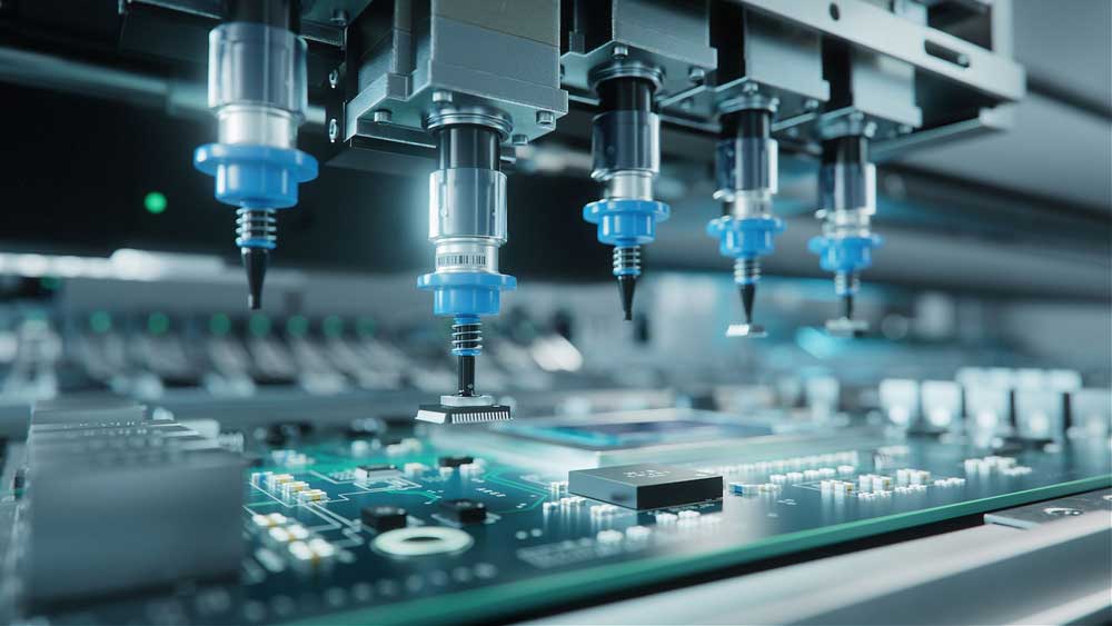
When placing the SMT components on the board, machine inaccuracies can cause one terminal to lie further into the pad than the other side.
This will lead to uneven wetting forces during reflow, making the side that lies further into the pad to be pulled more and lift the other side.
A pick-and-place machine at work
Improper Pad Design
Improper solder pad design refers to several aspects. These include being too far apart, having too many copper tracks connecting to one pad, or via-in-pads.
It can also include having different track widths or a plated-through hole/large copper area too close to one pad.
Legend/Silkscreen Between Pads
Although the silkscreen is an extremely thin layer, remember tiny SMT components lie almost flat on the PCB.
Therefore, a tiny legend layer between the solder pads can raise the SMT device slightly, causing it to bend to one side when placed. This bending can cause the side with little contact to rise during reflow.
Imbalanced Reflow Thermal Profile
This imbalance usually occurs when an assembler fails to preheat the board sufficiently during the reflow process. It can make the joints heat up unevenly, resulting in tombstoning.
Poor-quality reflow machines or large ones that handle multiple boards simultaneously can distribute the heat unevenly inside, forming uneven wetting on the pads.
Incorrect Solder Paste Deposition
Solder paste deposition inconsistency occurs when a poor-quality stencil prints or applies more solder on one side.
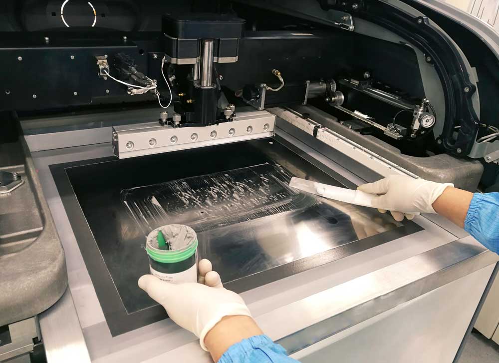
Applying solder paste on a PCB via a stencil
This flaw can cause tombstoning in two ways. First, the side with more solder might take more time to fully melt, resulting in a melting time difference that causes the other side to lift it.
In the second scenario, if the wetting speed time difference is minimal, the side with more solder will exert more pulling force that might be enough to lift the other side.
Different Solder Paste Compositions
Solder is an alloy containing different metals. If you apply solder with different compositions on each pad, the alloys will melt at different temperatures, meaning one side will wet at a shorter time. This issue is not as common but can occur if you’re using both Leaded and Lead-free solder paste.
Component Design
Thick components are more prone to tombstoning because they have a larger terminal surface area for pulling if the solder melts faster on one side. Those with uneven weight distributions or different thermal characteristics on each terminal are also more likely to tombstone.
Board or Component Oxidation
Solder pad or component terminal oxidation impedes wetting due to the oxide layer above the metal. This can increase the wetting time on one side, increasing the probability of tombstoning.
Board or Component Warpage
A warped component or PCB can cause one terminal to lose or have minimal contact with the solder pad. This allows the solder in the other to exert more pulling force that lifts the device.
Nitrogen Presence
Nitrogen has some benefits in the soldering process, such as reducing beading. However, it is a recipe for tombstoning because the gas enhances wetting.
If it is more available on one pad or terminal, it will make that side wet faster and build up enough force to lift the other.
Solder Mask or PCB Quality
Poorly stored PCBs can absorb moisture, which can try to escape through the pad area as vapor during reflow. Poor-quality solder masks can also have solvents that can escape through the pad area when hot, creating the tombstone effect.
Narrow Pad Pitch
If the solder pads are too close together, solder paste can easily slide between them during printing. This will cause the component to float above the paste and cause imbalanced pulling forces on the terminals during reflow.
How To Prevent Tombstoning During PCB Assembly
Optimize the Reflow Thermal Profile
It is paramount to optimize and maintain a balanced reflow thermal profile to ensure the joints heat evenly. Remember to preheat the board first when it enters the reflow oven and ensure the oven applies even heating to all PCB parts.
Optimize Solder Paste Deposition
The primary device used in solder paste deposition is the stencil and it has a significant role to play.
It must match the component’s land pattern design, lie flat on the board, and not be too thick. So stencil design is critical, whereby engineers should check its aperture size, spacing, and shape.
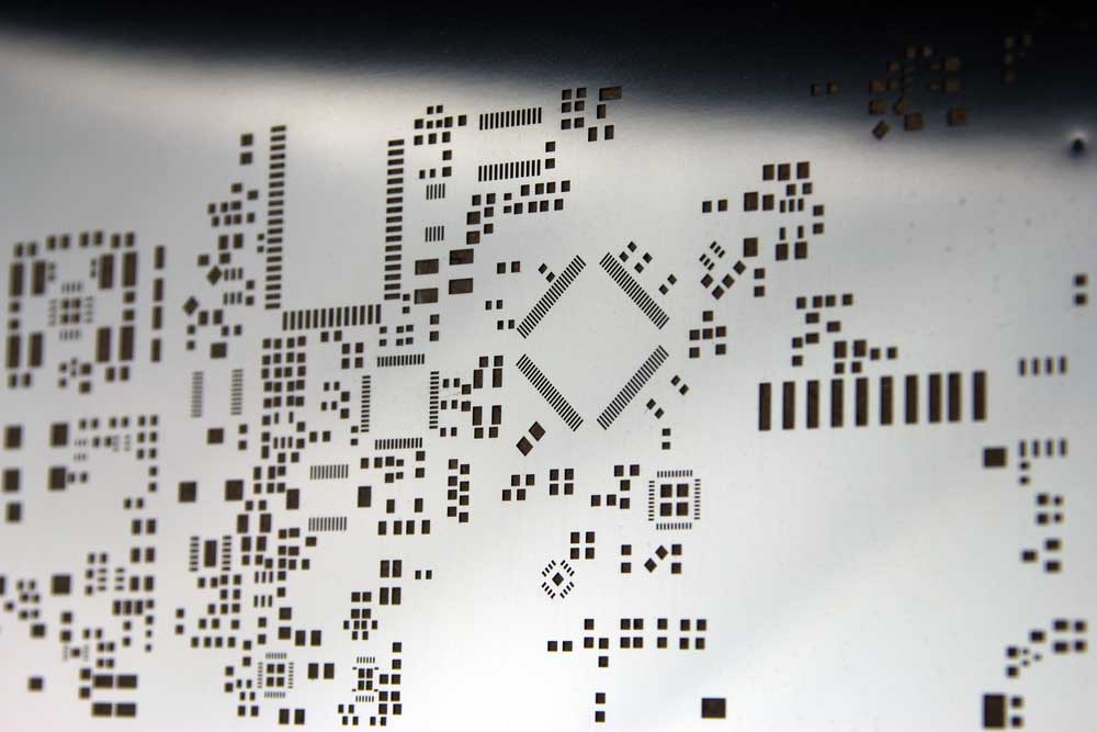
A laser-cut stainless-steel stencil
Check the Component Design
Component selection is also critical to minimizing tombstoning. These SMT devices should have equal terminal sizes and a balanced weight on both ends.
Check the Component Placement
An automated assembly line must have precise pick-and-place machines with high-quality vision systems to prevent inaccurate component positioning on the pad and solder.
Consider Changing the PCB Finish
The standard surface finish for most PCBs is Hot Air Solder Leveling. However, it can cause an uneven surface finish on the pads, which can affect wetting and cause tombstoning.
So, you might want to consider other surface finishes, like immersion gold or tin.
PCB ENIG surface finish
Ensure the Pads and Inner Copper Layers Have a Proper Design
The pad size and design should be consistent to prevent uneven heating. This design optimization should go further into the traces, where each pad should have roughly the same number of connections to have equal “cooling sinks.” Also, avoid placing some pads near large copper areas.
Ensure the Solder Mask is Thin
If the solder mask thickness rises above the land patterns, it can hamper the flow of solder as it melts.
The result will be inconsistencies when covering the component’s terminal or a weak joint. It is good practice to keep this layer thin and lower than the pads.
Do Regular Process Audits and Implement Quality Control
You need to monitor and calibrate the design, manufacturing, and assembly steps that can cause tombstoning over time to eliminate this issue.
At the same time, you should implement the required quality control measures to prevent or detect this occurrence early on. These measures include visual and automated optical inspection.
How OurPCB Can Help You
As you can see, the tombstone phenomenon has several root causes that should be fixed as early as in the PCB layout/design process. At OurPCB, we can help you bury your tombstoning defects in eternity (pun intended) by helping you out in all the production phases, beginning with design.
Our design rule checks are thorough and we have experts who’ll inform you of your board layout flaws. They will also give you improvement recommendations to avoid this defect later on.
During PCB manufacturing and storage, we have high-quality equipment that will prevent PCB warpage and moisture absorption, which can cause tombstoning.
Assembly is the most critical part, and before we begin this process, we will source high-quality components that perform and are balanced on weight and terminal design.
Our stencil production quality is also top-notch. Additionally, we only use machines from reputable suppliers like Yamaha and Siemens on the assembly lines (pick-and-place, reflow ovens, etc.).
Lastly, all our assembled boards undergo rigorous checking and testing to ensure they leave our factories defect-free. Over time, we have calibrated our systems to produce the best quality PCBAs, so you can rest assured that we’ll deliver tombstone-free products.
Contact us if you need help with PCB design, manufacturing, and assembly that is free from any defects, and we’ll be in touch ASAP.
Special Offer: Get $100 off your order!
Email [email protected] to get started!