Laser Direct Imaging is a relatively new technology in the PCB industry. It has an advantage over other, more traditional technologies by improving the speed of the whole PCB fabrication process, especially in PCB prototyping. Contact OurPCB to help you choose the best imaging technology for your PCBs!
Contents
- What is Laser Direct Imaging (LDI)?
- How Does Laser Direct Imaging Work?
- Where is Laser Direct Imaging used in PCB Manufacturing?
- High-Density Interconnect (HDI) PCBs
- Flexible PCBs
- Rigid-Flex PCBs
- Rapid Prototyping
- Solder Mask Application
- Silkscreen Layer Printing
- Inner Layer Imaging
- Outer Layer Imaging
- What are the Different Types of PCB Imaging Techniques?
- 1. Photolithography
- 2. Laser Direct Imaging
- 3. Inkjet Printing
- 4. Screen Printing
- 5. 3D Printing
- 6. Dry Film Imaging
- What is the Difference Between Positive and Negative Images?
- Positive Image
- Negative Image
- Solder Mask Solutions in PCB Fabrication
- Function of Solder Mask
- Types of Solder Mask Materials
- Application Methods for Solder Mask
- LDI in Solder Mask Application
- Benefits of Using LDI for Solder Mask
- What is the Laser Direct Imaging Process?
- What are the Advantages of Laser Direct Imaging?
- Precision
- Accuracy
- Flexibility
- Speed
- Cost-Effectiveness
- Environmentally Friendly
- High Resolution
- Improved Yield and Reliability
- Faster Time-to-Market
- What are the Challenges of Laser Direct Imaging?
- High Initial Investment
- Specialized Materials
- Process Complexity
- Limited Throughput for Large Panels
- Maintenance and Calibration
- When Should You Use Laser Direct Imaging?
- High-Density Interconnect (HDI) Boards
- Prototyping
- Complex PCB Designs
- Miniaturized Electronics
- Time-Sensitive Projects
- Laser Direct Imaging FAQs
- Can LDI Be Used for Both Rigid and Flexible PCBs?
- Does LDI Improve the Reliability of High-Density Interconnect (HDI) Boards?
What is Laser Direct Imaging (LDI)?
Laser Direct Imaging (LDI) is a technology used in printed circuit board (PCB) manufacturing. It uses a computer-controlled, highly focused laser beam to transfer circuit patterns directly onto a photoresist-coated PCB.
Unlike traditional methods that use physical photomasks and UV light, LDI simplifies the process by directly imaging the design onto the board. This technique has higher precision, better alignment, and the ability to handle more complex and dense designs, so it’s an excellent choice for modern electronics manufacturing
How Does Laser Direct Imaging Work?
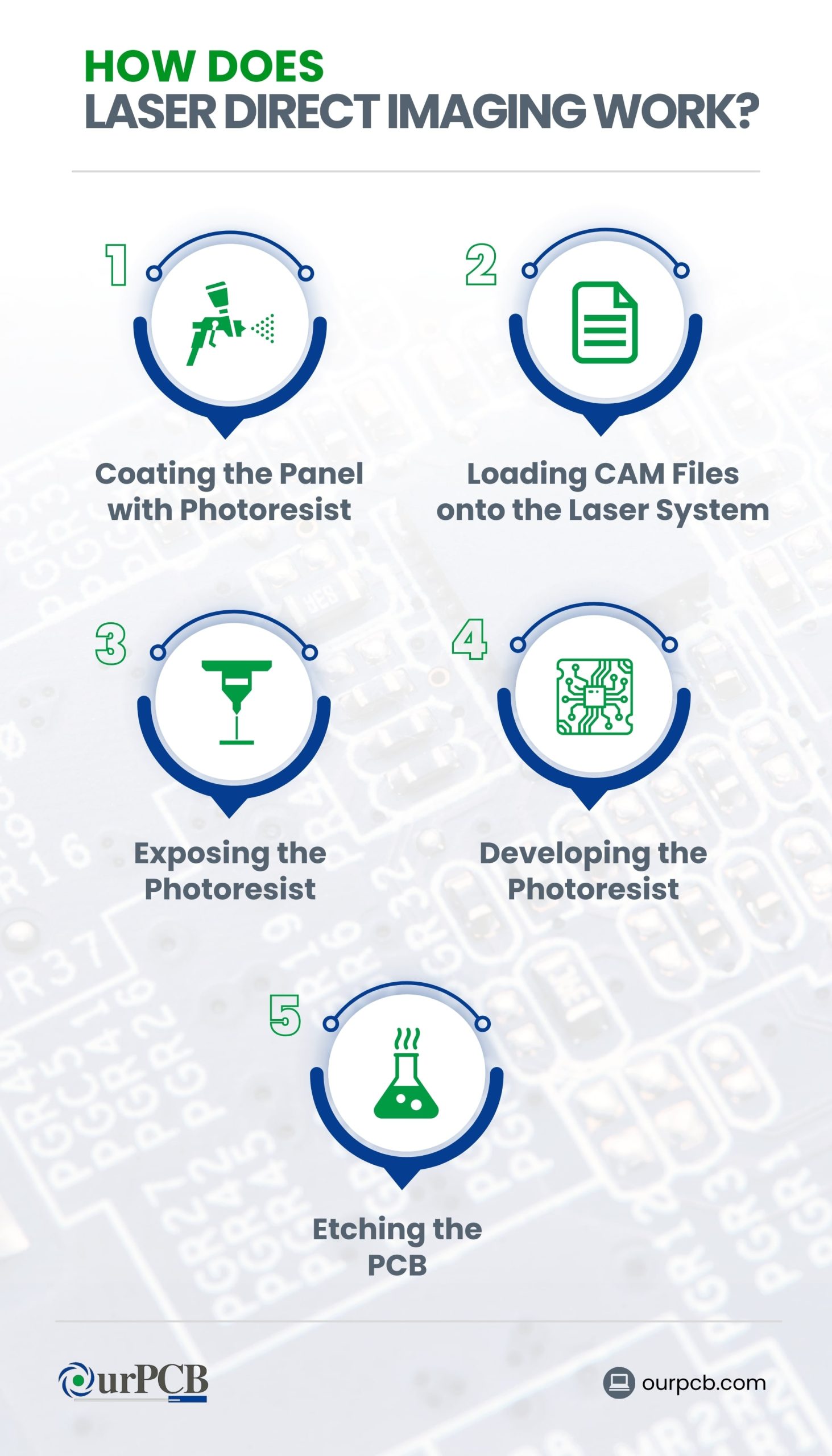
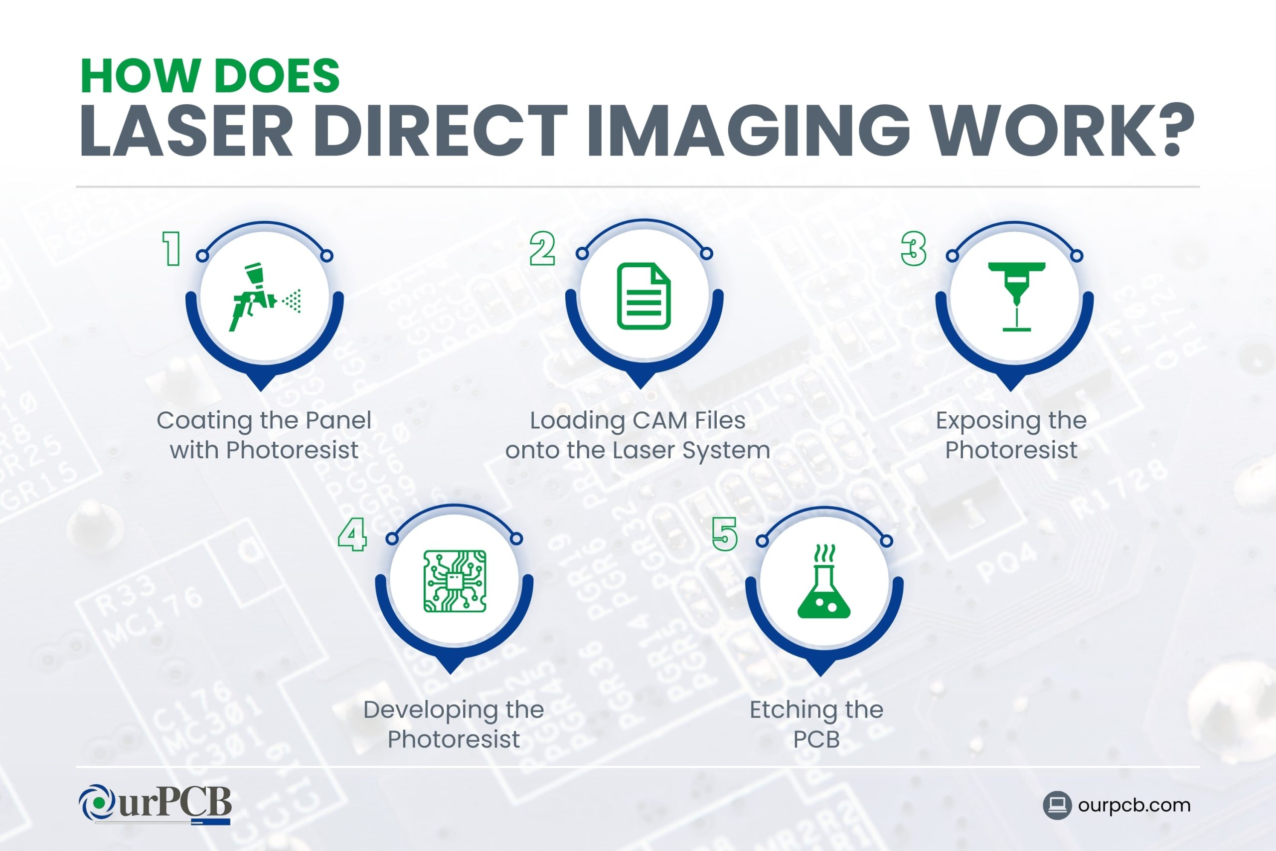
LDI works like a high-tech printer for circuit boards. It uses a powerful laser beam to create the circuit pattern directly on the board, instead of relying on traditional film masks.
- Coating the Panel with Photoresist: The PCB panel is coated with a photo-sensitive material known as photoresist. This layer reacts to light, making it possible to create detailed patterns.
- Loading CAM Files onto the Laser System: The computer-aided manufacturing (CAM) files, which contain the design of the circuit, are loaded onto the laser system. These files guide the laser in creating the circuit pattern.
- Exposing the Photoresist: A computer-controlled laser beam is used to directly expose the photoresist-coated panel. The laser follows the pattern defined by the CAM files, hardening the photoresist where the circuit paths will be.
- Developing the Photoresist: After exposure, the panel is developed, which removes the unexposed photoresist, leaving behind the hardened pattern.
- Etching the PCB: The areas not protected by the hardened photoresist are etched away using an acid solution, revealing the circuit pattern on the copper layer of the PCB.
Where is Laser Direct Imaging used in PCB Manufacturing?
Laser Direct Imaging is used in various stages of PCB manufacturing, particularly where high precision and flexibility are needed.
High-Density Interconnect (HDI) PCBs
LDI is a favorite for manufacturing HDI PCBs, which have very fine lines and spaces, multiple layers, and complex structures. The precision of LDI makes it ideal for these high-density designs where traditional photolithography might fall short.
Flexible PCBs
Flexible PCBs
are used in devices where space is tight, and the circuit needs to bend, as in medical devices and wearables. LDI allows for quick design changes and fast prototyping, which is helpful for custom designs and small production runs. This flexibility and speed are hard to achieve with older methods that need new masks for each change.
Rigid-Flex PCBs
combine rigid and flexible circuits into one board, needing precise alignment. LDI ensures they align properly and that both parts of the PCB are accurately connected.
Rapid Prototyping
LDI is particularly beneficial for prototyping, allowing for rapid design changes without the need for new photomasks. This speeds up the development process and reduces costs, making it ideal for small production runs and frequent design iterations.
Solder Mask Application
Solder mask
(or soldermask) is a protective layer that covers most of the copper, leaving only the pads and connection points exposed. LDI precisely defines the solder mask pattern, preventing solder bridges between components during assembly and giving you a clean, professional look.
Silkscreen Layer Printing
LDI can also be used to create the silkscreen layer, which has the labeling and identification references for polarity markings, test points, and other information to help in PCB assembly and testing.
Inner Layer Imaging
PCBs often have multiple layers sandwiched together. LDI is used to create the intricate circuit patterns on these inner layers, which are hidden within the board. This gives you accurate trace placement and minimizes signal interference.
Outer Layer Imaging
The outer layers are where components are soldered onto the board. LDI helps with precise imaging for these layers, especially important for high-density boards with fine-pitch components. This accuracy helps prevent shorts and open circuits, making sure the board functions correctly.
What are the Different Types of PCB Imaging Techniques?
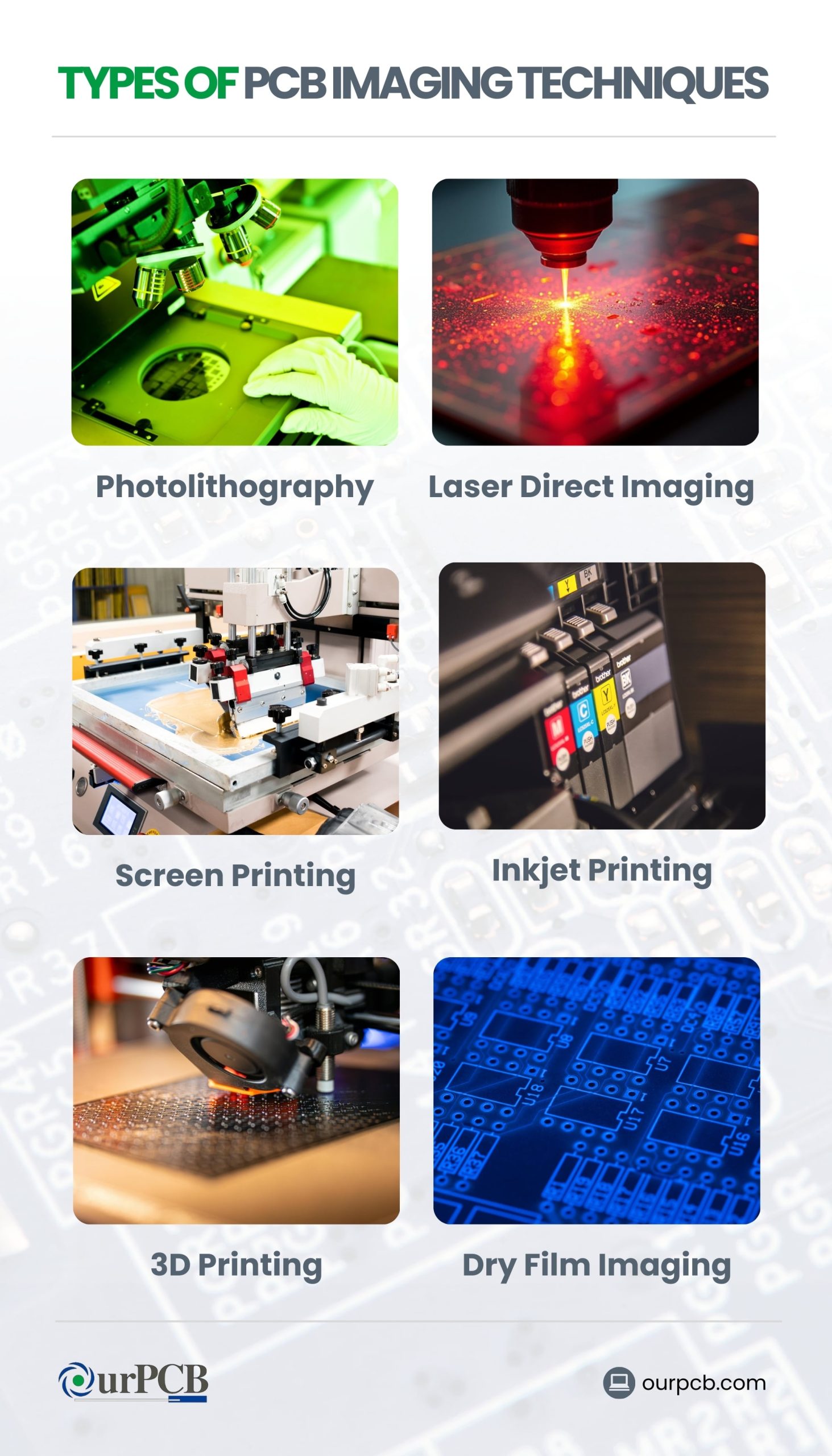
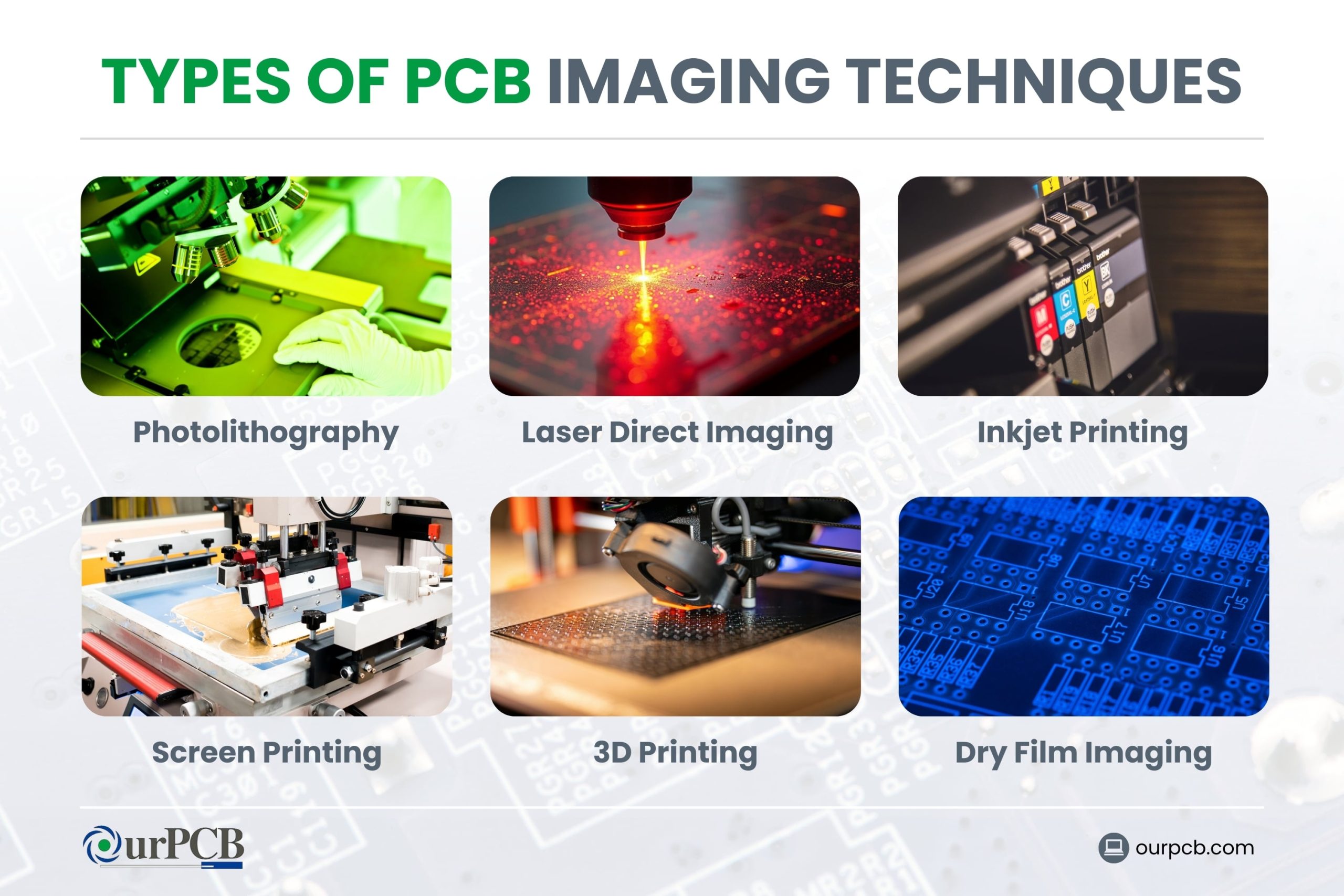
1. Photolithography
Photolithography is a widely used technique for PCB imaging. It involves coating the PCB with a photosensitive material called photoresist. The board is then exposed to ultraviolet (UV) light through a mask that contains the desired circuit pattern.
The exposed areas of the photoresist harden, while the unexposed areas are removed, revealing the underlying copper for etching.
2. Laser Direct Imaging
LDI is a more advanced technique that uses lasers to directly expose the photoresist on the PCB. This method doesn’t need a physical mask, making it more flexible and capable of producing higher-resolution patterns. LDI is ideal for complex and high-density PCB designs.
3. Inkjet Printing
Inkjet printing for PCB imaging uses an inkjet printer to apply conductive ink directly onto the PCB substrate. This method is cost-effective and suitable for rapid prototyping and small production runs. However, it may not achieve the same precision as photolithography or LDI for very fine details.
4. Screen Printing
Screen printing is a traditional method where a stencil or screen with the circuit pattern is used to apply conductive ink or paste onto the PCB substrate. This technique is commonly used for creating simple and less detailed PCB designs. It’s cost-effective for large-scale production but less suitable for intricate patterns.
5. 3D Printing
, or additive manufacturing, involves using a 3D printer to build up layers of conductive and insulating materials to form the PCB. This method offers great flexibility and can create complex multilayered PCBs, but it’s still in the developmental stages for widespread industrial use.
6. Dry Film Imaging
Dry film imaging uses a photosensitive dry film that’s laminated onto the PCB substrate. The film is exposed to UV light through a photomask, and the exposed areas are developed to reveal the circuit pattern. This method is known for its high resolution and is commonly used in professional PCB manufacturing.
What is the Difference Between Positive and Negative Images?
The terms “positive” and “negative” refer to how the circuit pattern is represented on the imaging layer.
Positive Image
In a positive image, the areas of the PCB that will be covered with copper are represented by dark areas on the imaging layer (photoresist or dry film). The laser or UV light exposure hardens these dark areas, protecting them during the etching process. The unexposed areas are washed away, leaving the copper traces behind.
Negative Image
In a negative image, the areas of the PCB that will be covered with copper are represented by clear (or transparent) areas on the imaging layer. The laser or UV light exposure hardens the surrounding areas, leaving the clear areas unprotected. During etching, these unprotected areas are removed, resulting in the copper traces from the design.
Special Offer: Get $100 off your order!
Email [email protected] to get started!
Solder Mask Solutions in PCB Fabrication
Function of Solder Mask
- Protection: Solder mask acts as a primary defense against environmental factors like moisture, dust, and chemicals. This protection safeguards the copper traces from oxidation and corrosion, making sure the PCB lasts a long time.
- Insulation: It prevents unintended electrical connections (short circuits) between adjacent conductive areas during soldering or operation.
- Visibility: Solder mask enhances the visual contrast between components and traces, helping with inspection, troubleshooting, and repair. It also contributes to the overall professional appearance of the PCB.
Types of Solder Mask Materials
- Epoxy Liquid Photoimageable (LPI): Applied as a liquid and cured with UV light, suitable for high-density PCBs but can be expensive.
- Dry Film Photoimageable (DFP): Laminated onto the PCB surface, offering high chemical resistance, ideal for high-temperature and multilayer boards.
- Top-Side vs. Bottom-Side Materials: Different materials may be used depending on thermal resistance and chemical exposure needs.
Application Methods for Solder Mask
Screen Printing
A stencil is used to apply the solder mask onto the PCB. This method is suitable for high-volume production and provides good control over thickness.
Curtain Coating
The solder mask is poured over the PCB in a continuous curtain. It offers high throughput and even coverage, but may not be suitable for complex designs.
Spray Coating
The solder mask is sprayed onto the PCB. This method is flexible and can accommodate various PCB sizes and shapes. However, it needs careful control to achieve uniform thickness.
LDI in Solder Mask Application
LDI is an emerging technology in the PCB fabrication process that’s revolutionizing solder mask application. Instead of using traditional phototools (films) to expose the solder mask, LDI directly exposes the solder mask material using a laser beam guided by digital data.
Benefits of Using LDI for Solder Mask
- Precision: Eliminates phototool errors, leading to higher accuracy and registration
- Flexibility: Enables rapid design changes without new phototools
- Cost-Effective: Eliminates phototool fabrication and storage costs
- Eco-Friendly: Reduces chemical usage compared to traditional methods
- High Resolution: Achieves finer lines and details, ideal for complex designs
What is the Laser Direct Imaging Process?
- Surface Preparation: The PCB surface is scrubbed to remove oxide layers and contaminants, making sure the photoresist adheres properly.
- Photoresist Application: A layer of photoresist is laminated onto the PCB. This photosensitive material is essential for the imaging process.
- Load Design Files: The design files (CAM files) are loaded into the LDI system, guiding the laser to create the circuit pattern.
- Laser Exposure: The laser directly exposes the photoresist according to the design, creating the circuit pattern on the PCB.
- Etching: The unexposed areas of the photoresist are etched away, revealing the copper traces of the circuit pattern.
- Photoresist Removal: The remaining photoresist is stripped away, leaving only the desired circuit pattern on the PCB.
- Drying: The PCB is dried to finalize the circuit pattern and prepare it for further processing or assembly.
What are the Advantages of Laser Direct Imaging?
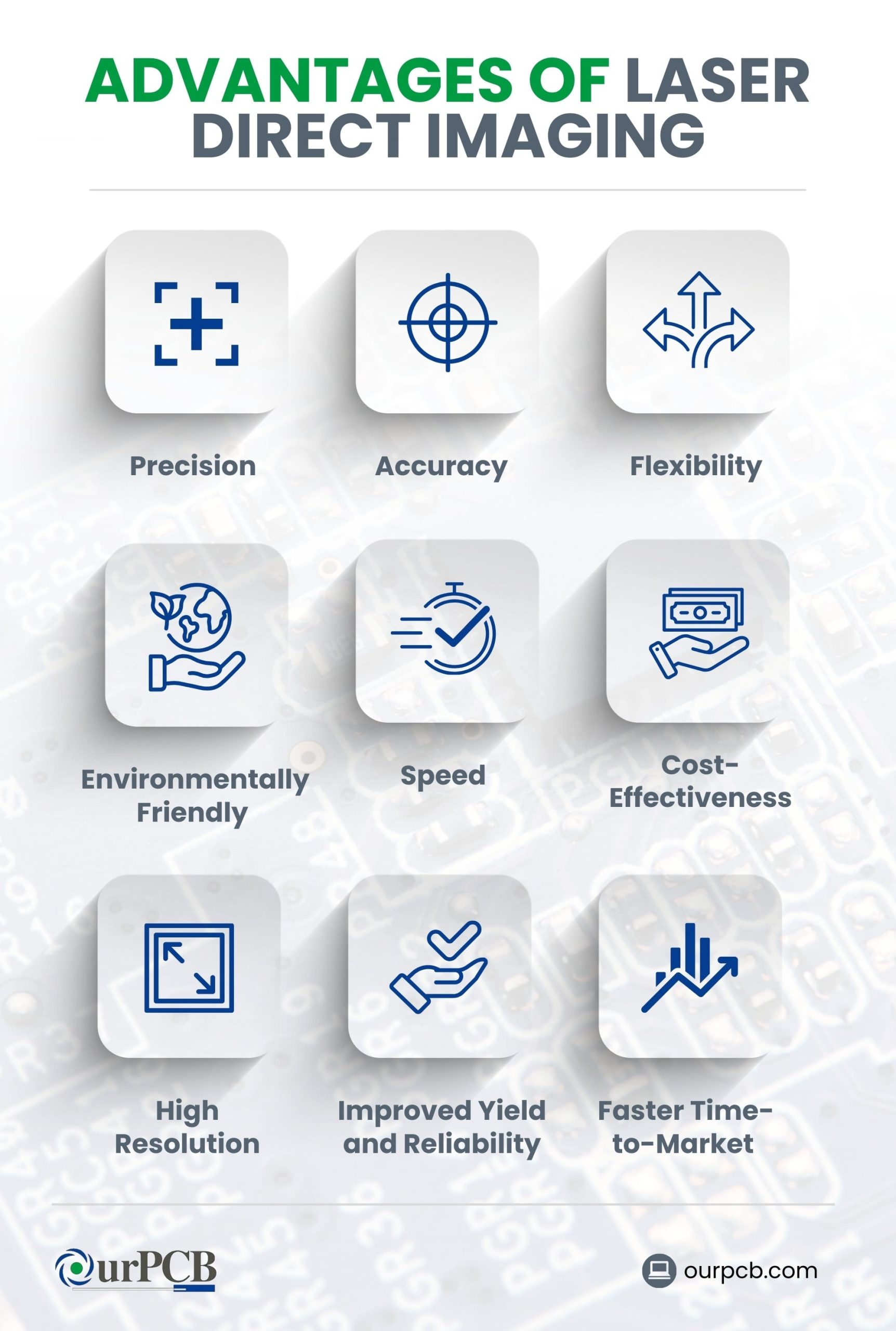
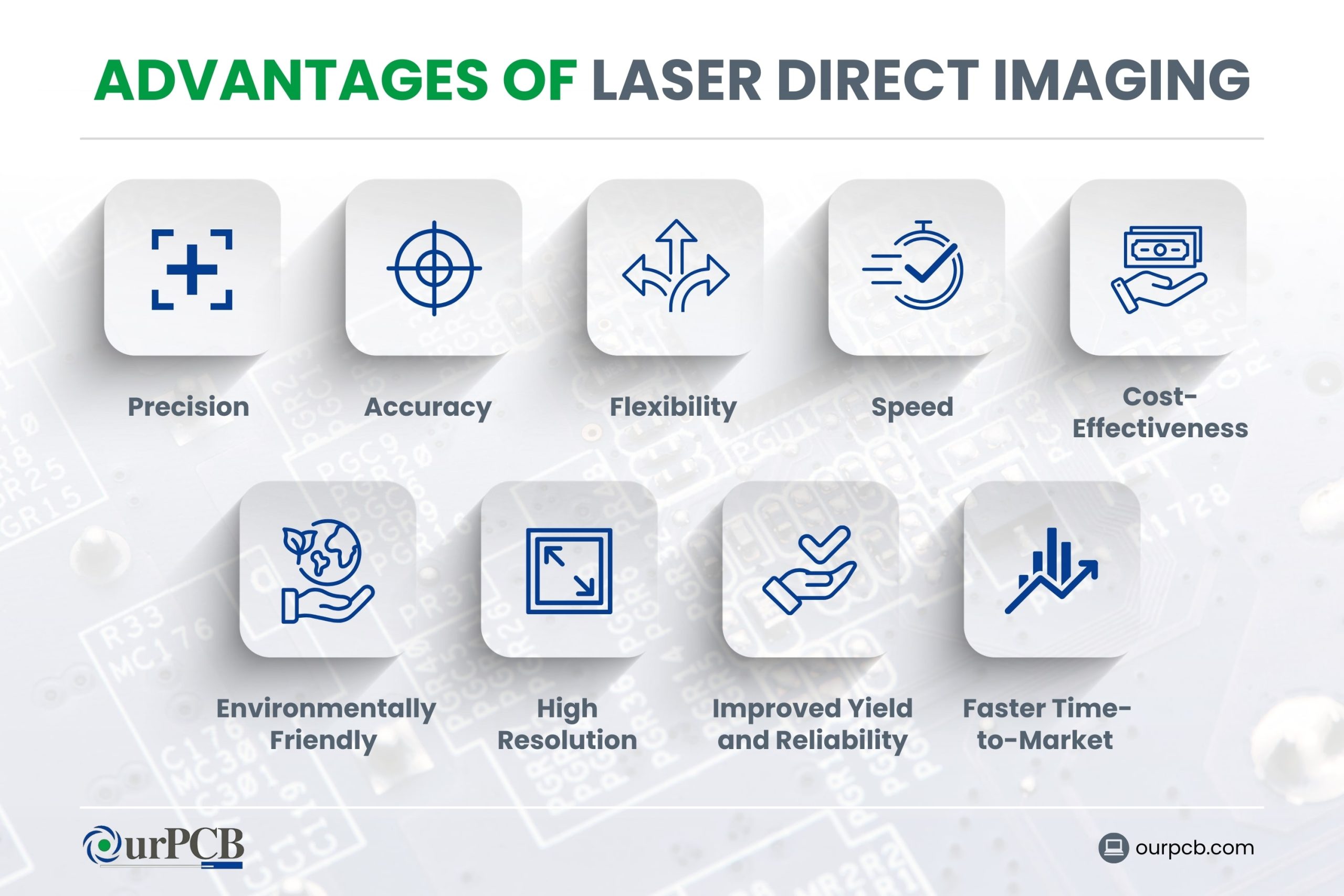
Precision
Laser Direct Imaging (LDI) eliminates possible errors introduced by physical phototools, resulting in highly accurate and consistent patterns. This high level of precision is a must for modern PCB designs with tight tolerances.
Accuracy
The laser precisely follows digital instructions, for accurate registration and alignment of features. This reduces misalignment issues that tend to take place in traditional methods using photomasks.
Flexibility
LDI enables rapid design changes and modifications without the need for creating new phototools. This flexibility is particularly handy for prototyping and small production runs, allowing for quick adjustments to designs.
Speed
By streamlining the time-consuming steps in traditional phototool creation and alignment, LDI leads to faster production cycles. Digital data can be directly used to produce PCBs, speeding up the manufacturing process quite significantly.
Cost-Effectiveness
LDI eliminates the costs of phototool fabrication, storage, and maintenance. Although the initial investment in LDI equipment can be high, the overall production costs are lower, making it a cost-effective solution.
Environmentally Friendly
LDI uses fewer chemicals than traditional phototool development processes. The dry laser exposure process minimizes the environmental impact, so it’s a more sustainable option.
High Resolution
LDI achieves finer lines, details, and smaller features, excellent for complex and high-density designs. This high resolution is important for advanced PCBs, like those used in HDI applications.
Improved Yield and Reliability
The precise and consistent patterns created by LDI lead to higher yields and improved reliability of the final products.
Faster Time-to-Market
The combination of speed, flexibility, and accuracy provided by LDI means faster product development and quicker time-to-market.
What are the Challenges of Laser Direct Imaging?
High Initial Investment
LDI systems can be expensive compared to traditional phototool-based equipment. The initial investment may be a barrier for smaller PCB manufacturers or those with limited budgets.
Specialized Materials
LDI uses specialized photosensitive materials (resists and solder masks) that are compatible with specific laser wavelengths and exposure parameters. These materials may be more expensive than traditional materials.
Process Complexity
Achieving top results with LDI needs careful process optimization. This includes factors like adjusting laser power, exposure time, and other parameters to make sure you get the image quality and resolution you want. It may be a learning curve for operators.
Limited Throughput for Large Panels
LDI systems may have lower throughput compared to some high-volume photolithography methods, especially for very large panels. This should be a consideration for high-volume production environments.
Maintenance and Calibration
LDI systems need regular maintenance and calibration to keep up their high level of accuracy and performance. This can add to the overall operating costs.
When Should You Use Laser Direct Imaging?
High-Density Interconnect (HDI) Boards
The experts at OurPCB can confirm that LDI is perfect for HDI boards requiring precise microvias and fine lines. If you need sub-micron accuracy for intricate, multilayer structures, use LDI.
Prototyping
One of the biggest advantages of LDI is that it allows for rapid design changes without physical photomasks. This streamlined approach means it’s ideal for prototyping and short production, lowering both time and costs.
Complex PCB Designs
LDI supports detailed patterns and narrow trace widths, which makes a big difference for advanced and complex PCB designs that demand high performance.
Miniaturized Electronics
For small, densely packed PCBs in modern electronics, LDI has a high level of precision. This is important for compact and miniaturized components.
Time-Sensitive Projects
LDI speeds up production by getting rid of time-consuming steps like photomask creation. It’s a great choice for projects with tight deadlines.
Laser Direct Imaging FAQs
Can LDI Be Used for Both Rigid and Flexible PCBs?
Yes, Laser Direct Imaging (LDI) can be used for both rigid and flexible PCBs. It’s known for high precision and flexibility, so it’s suitable for producing intricate patterns on various substrates, including those used in rigid-flex designs.
Does LDI Improve the Reliability of High-Density Interconnect (HDI) Boards?
Yes, Laser Direct Imaging (LDI) improves the reliability of High-Density Interconnect (HDI) boards by allowing for precise microvia formation and accurate alignment.
Back to top: Laser Direct Imaging
Special Offer: Get $100 off your order!
Email [email protected] to get started!