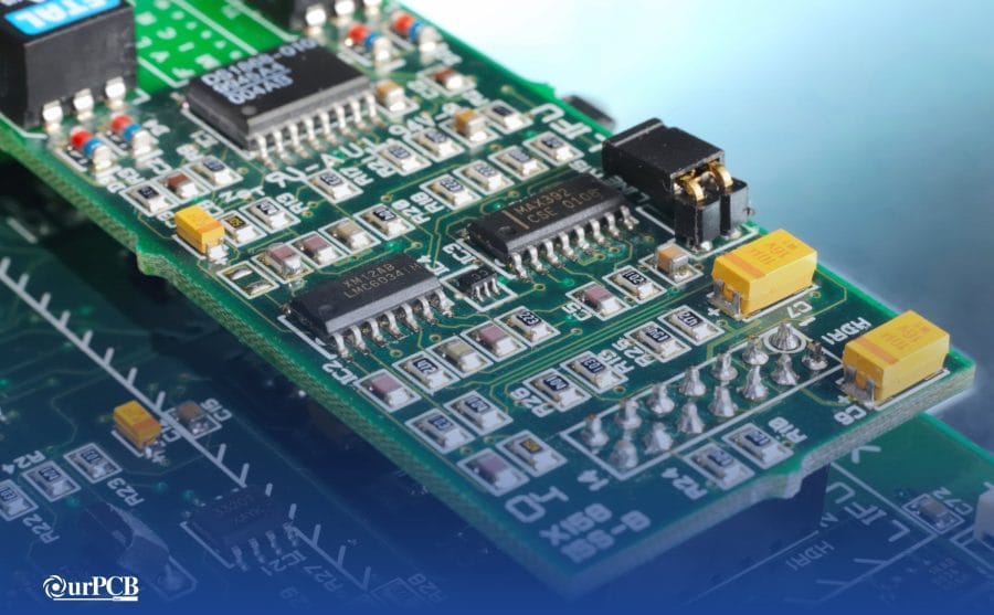
The electrical return/return current path is one of the fundamental aspects to consider when designing a circuit.
This aspect is even more vital when designing PCBs because they feature tiny current paths compressed into a compact package.
And as the demand for tiny PCBs grows, the operating current/voltage in these circuits has reduced dramatically.
These compact designs present a challenge when making current return paths, which we’ll look at below.
Read on to learn more about this topic and how to design a return current path in PCBs.
Contents
- What Is Return Current?
- DC Return Current Path
- AC/Pulse Signal Return Current Path
- Capacitive vs. Inductive Return Current Path
- Low Frequencies (1 KHz - 100 KHz)
- High Frequencies (>10 MHz)
- Medium-High Frequencies (500 KHz - 1 MHz)
- How To Design a Return Current Path in a PCB
- Place the Ground Plane in the Adjacent Layer
- Define the Analog and Digital Board Sections
- Position a Grounded via Next to a Signal via During Layer Transitions
- How To Confirm This Current Flow Path
- Wrap Up
What Is Return Current?
Most people compare the current flow in a circuit with water flowing in a pipe for easy visualization and understanding.
So this current must return somewhere to the power source’s zero potential terminal to complete the circuit.
The return current is this electricity linking back to the source after powering circuit components.
However, that is not how electrical circuits work.
This visualization of flowing electrons might lead to incorrect reasoning about the operations inside electrical circuits.
Electricity does not flow like water.
Instead, the charges in the conductor create magnetic fields around it, which move the energy around the circuit.
These fields don’t move inside the conductor; they travel around it, meaning they can interact or interfere with other parts of the circuit.
Therefore, the return current path can shift depending on the signal’s frequency and associated impedance.

A radio frequency PCB on a Smith chart for impedance matching
DC Return Current Path
With direct current, the energy flows continuously in one direction. So the return current path is the one with the least resistance.
Therefore, the current will flow in a direct, straight line back to the power supply.
For instance, let’s consider a circuit where a 5V power supply flows through a top-layer conductor into an IC.
This board has an interior ground plane with a substrate separating the two layers.
A via connects the two to complete the circuit from the IC ground pin.

A PCB with multiple via holes
The current leaving the IC goes into the ground plane through the via and back to the 5V source through another via.
The substrate provides insulation and capacitance between the top and inner conductors.
So the DC experiences infinite reactance (hence infinite impedance) between the top and inner layer.
Therefore, it does not move through the substrate via lumped capacitance.
And once it goes into the ground plane, it follows the least resistance path.
AC/Pulse Signal Return Current Path
The dynamics differ when dealing with AC, digital, or analog frequency signals.
Since these are time-varying signals, the voltage, and current levels change with time.
Still using the example above, the electric signal can induce a current in the substrate via lumped capacitance.
This displacement current will then travel to the ground plane in the inner layer.

Signal traces on a PCB
.
So the return current won’t come from the IC.
Instead, the circuit will create this current in the ground plane.
Also, the resistance won’t change with frequency.
But the reactance generated by the capacitance formed in the substrate will depend on the frequency.
So the return current will concentrate more under the signal trace because it is the path of minimal reactance.
Special Offer: Get $100 off your order!
Email sales@ourpcb.net to get started!
Capacitive vs. Inductive Return Current Path
Circuit impedance can either be reactive or resistive, with the former being dependent on frequency.
The latter is independent of frequency.
And although circuits might not have inductors or capacitors, you should model transmission lines as RLC circuits.
Some parasitic capacitance always occurs in the substrate between the top-layer conductor and the inner ground layer.
But parasitic inductance occurs due to the closed-loop conductor in the circuit.

A PCB with a bottom layer ground plane
A combination of parasitic charges and the conductor’s DC resistance creates the impedance experienced by signals traveling through the circuit.
So the return current path will experience these charges, but in different strengths depending on the frequency.
Low Frequencies (1 KHz - 100 KHz)
Pulses propagating at low frequencies return the current through the path of least resistance (like DC).
Because of the weak parasitic capacitance, this current gets inductively induced as a loop around the circuit.
So it creates a straight path between the ground and the source.
High Frequencies (>10 MHz)
Once you transmit high-frequency signals over 10 MHz, parasitic capacitance between the source and reference plane will dominate the circuit.
So the return current path will form underneath the upper signal trace because it is the path of minimal reactance.
Medium-High Frequencies (500 KHz - 1 MHz)
The current return splits between the two paths if transmitting the signal between the low and high frequencies.
Some electrical current goes via a straight line back to the source, while the rest travels under the signal trace.

The electrical waveform of a measured digital signal (high-frequency currents)
How To Design a Return Current Path in a PCB
An unpredictable return current path can cause ground noise, interfering with signal lines in the circuit.
So design the PCB in such a way that creates a stable and predictable current return path.
Here’s what you need to consider.
Place the Ground Plane in the Adjacent Layer
Placing an adjacent reference plane is the best way to create a predictable return path with low or high-frequency signals.
If not in this plane, the return path will form due to capacitive or inductive coupling to the nearest ground plane.
The capacitive and inductive coupling creates charges that cause interference in the signal layers.
Define the Analog and Digital Board Sections
If designing a circuit board that handles analog and digital signals, define the two sections first.
The best way to specify them is to position them on different board sections.
And avoid placing one above the other because the signals will cause interference.
Place the circuits on different sides, then place a single return current path between them.
You can use a different ground plane for each signal type, but this design can create capacitive coupling.
The analog and digital signals can interfere with the other’s ground layer.
So you’ll have to design your board with separate parts to prevent interference.
Position a Grounded via Next to a Signal via During Layer Transitions
Depending on your circuit, you might have to transition a high-speed or high-frequency signal line between two PCB layers.
To minimize the loop inductance, always place a grounded via next to the signal-via.
Otherwise, the closest decoupling capacitor will provide the return current, creating high loop inductance.
How To Confirm This Current Flow Path
These return current path facts might not be easy to comprehend.
So we recommend doing simple tests to experiment with high and low-frequency signals.
You’ll need the following components.
- Function generator
- Coaxial cable
- 50Ω load resistor
- Oscilloscope
The power signal comes from the function generator, travels through the coaxial cable’s middle conductor, and into the load.
And we’ll connect a copper wire from the circuit load back to the power source’s low terminal.
Ensure you connect the circuit in a way that forms a coaxial cable loop to join the copper wire on both ends.

An oscilloscope probe assessing a circuit in the signal waveform
So the return current has two paths.
The first is through the copper wire, and the second is via the coaxial cable’s outer shield.
If you measure the current or voltage along the copper wire, you’ll notice variations as you adjust the signal frequency.
Low frequencies will give high current/voltage values.
But as you increase the frequency, the measurements will reduce.
The return current tends to go back via the cable’s outer shield because it is the path of minimal reactance.
Wrap Up
As you can see, electricity flow is critical in circuits because it brings forth different properties at varying frequencies.
So you need to follow the design tips listed above to create a PCB layout with zero interference.
And if you need any guidance, contact us.
We’ll be happy to help.
Special Offer: Get $100 off your order!
Email sales@ourpcb.net to get started!