Fabricating circuit boards is a complex process that requires you to factor in several variables to get the formula right. One of the defects that might arise is PCB delamination. This issue usually occurs due to manufacturing errors, but there are ways to prevent it. We will look closely at this defect to explain its causes, prevention measures, and repair steps. Read on to learn more!
Contents
- What is PCB Delamination?
- Blistering vs. Measling
- Causes of PCB Delamination
- Thermal Stress
- Moisture
- At What Temperature Does PCB Delamination Occur?
- Why Does the PCB Delaminate When Being Reflow Soldered?
- How Can You Tell Whether the PCB Is Harmed or PCB Delamination Has Occurred?
- Unusual Heating
- Crackling
- Corrosion
- Effects and Consequences of PCB Delamination
- Electrical Performance Issues
- Heat Dissipation Issues
- High Chances of Failure
- Reduced Lifespan
- Repair and Rework Difficulties
- Higher Manufacturing Costs
- Impaired Troubleshooting and Testing
- Preventive Measures and Mitigation Techniques
- Optimize the Design
- Pick the Best Material
- Optimize Manufacturing
- Implement Inspection and Quality Control Methods
- Analyze Failures and Implement Corrective Actions
- How To Prevent PCB Delamination
- Delamination Measurement Tests
- Delamination Repair Steps
- Steps
- Evaluation
- Wrap Up
What is PCB Delamination?
Delamination defines the physical separation of circuit board layers and can occur in inner or surface layers. The splitting can cause malfunctions in the internal layers that are difficult to pinpoint without thorough examination.
PCB inner layers
If viewed on an assembled printed circuit board or a bare one, delaminations might appear as broad, discolored or bubbling regions.
Blistering vs. Measling
Delamination has two related forms. Blistering is the partial separation that causes bubbles or gaps that look like blisters. The damage usually occurs in the production process.
On the other hand, measling refers to white spots on the PCB weave interior that indicate element destruction on the board. Small measling is tolerable, provided:
- It is not very frequent
- Does not bridge conductors and soldering eyes
Common causes of measling include errors in production and mechanical stress.
Causes of PCB Delamination
The two primary factors that lead to delamination include the following.
Thermal Stress
Repeated thermal stress before and after the assembly process can cause delamination, especially if the heat exceeds the glass transition temperature.
Manufacturers can prevent delamination by examining the wave soldering and reflow profile parameters to ensure the PCB base materials will not encounter excessive stress.
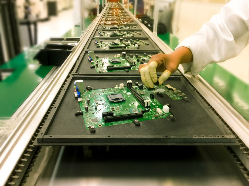
Circuit boards in an assembly line before wave soldering
Thermal-stress delamination might start in the interior layers without creating blisters or causing cracks on the surface layer. The manufacturer should use high-Tg board base materials if the board undergoes multiple soldering cycles, large thermal excursions later, or both.
Moisture
Moisture buildup in the PCB base layers is one of the most typical causes of delaminations. This moisture can contribute to CAF (Conductive Anodic Filamentation), where the water gets into electrochemical reactions that create tiny filaments. These filaments can bridge conductors, causing short circuits.
And this moisture will turn into steam when temperatures elevate during the processing steps later. The reflow soldering process, for instance, occurs at temperatures above 200°C. Such heat levels are well above the boiling temperature of the water and will convert the moisture into steam.
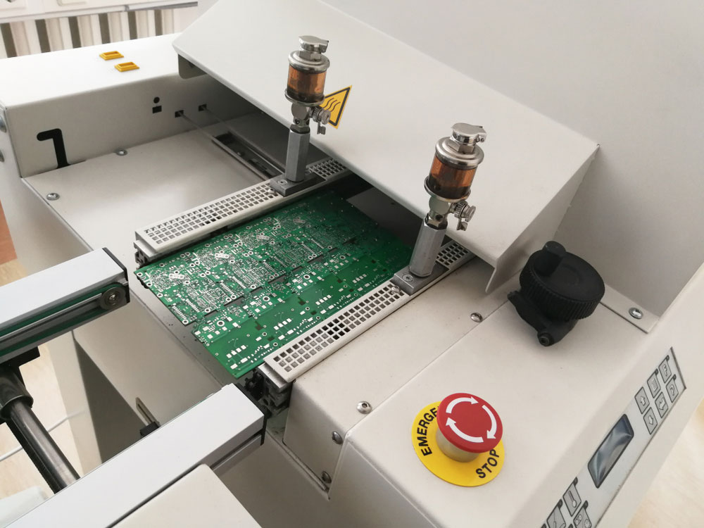
A PCB in a reflow oven machine to heat the solder paste
The pressure from this steam will interfere with curing and board pressing, ripping some sections apart. These separated parts or blisters might show immediately or later during subsequent thermal processing steps or large thermal excursions when the printed circuit board is used.
At What Temperature Does PCB Delamination Occur?
Delamination usually occurs when trapped moisture expands between the layers, and water can start expanding at temperatures as low as 176°F or 80°C.
Once the process sets off, factors like rapid temperature changes and thermal cycling can exacerbate the issue, causing further weakening of the adhesive bonds between the layers. This separation occurs due to differential contraction and expansion between the layers.
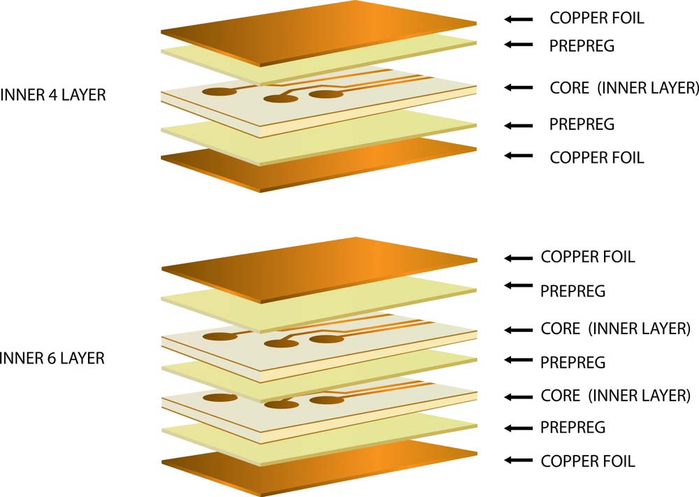
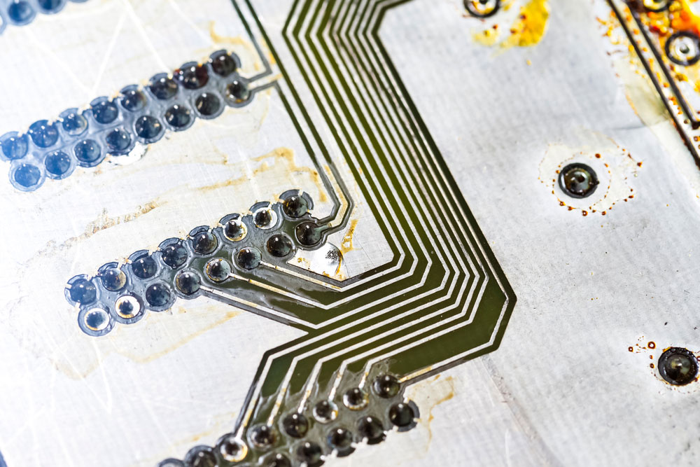
The layer-stack in multilayer printed circuit boards.
But the PCB layer materials can also determine if delamination occurs and the rate at which it occurs, especially if the board has different materials.
Why Does the PCB Delaminate When Being Reflow Soldered?
The reflow oven must reach temperatures between 240 and 250°C to melt Lead-free solder and form strong metal bonds with the electronic components. These temperatures are three times needed to expand trapped moisture between the layers to separate the layers.
This process takes about 60 seconds plus or minus 15, which is more than enough to do significant damage.
An infrared reflow soldering oven.
But this moisture doesn’t get in just before soldering; it penetrates the FR4 fiberglass material during and after manufacturing.
During manufacturing, some processes involve using wet chemicals, especially when making multilayer boards. These processes can leave liquids that can expand and delaminate the layers during reflow soldering.
But most of this moisture gets in after manufacturing. FR4 is water resistant, but it is hygroscopic. Without proper storage in a vacuum, the material can absorb water from the atmosphere, resulting in delamination when things get hot.
If you have doubts about the vacuum sealing, pre-bake the boards at a low temperature to push the vapor out.
Special Offer: Get $100 off your order!
Email [email protected] to get started!
How Can You Tell Whether the PCB Is Harmed or PCB Delamination Has Occurred?
PCB delamination might not be visible immediately after reflow soldering, but these signs will appear later when using the electronic device.
Unusual Heating
help with heat evacuation from hot components. If delaminated, this layered structure won’t be as effective and can make your board feel hot. Continued exposure to heat can peel the copper traces from the dielectric, causing short circuits and fires.
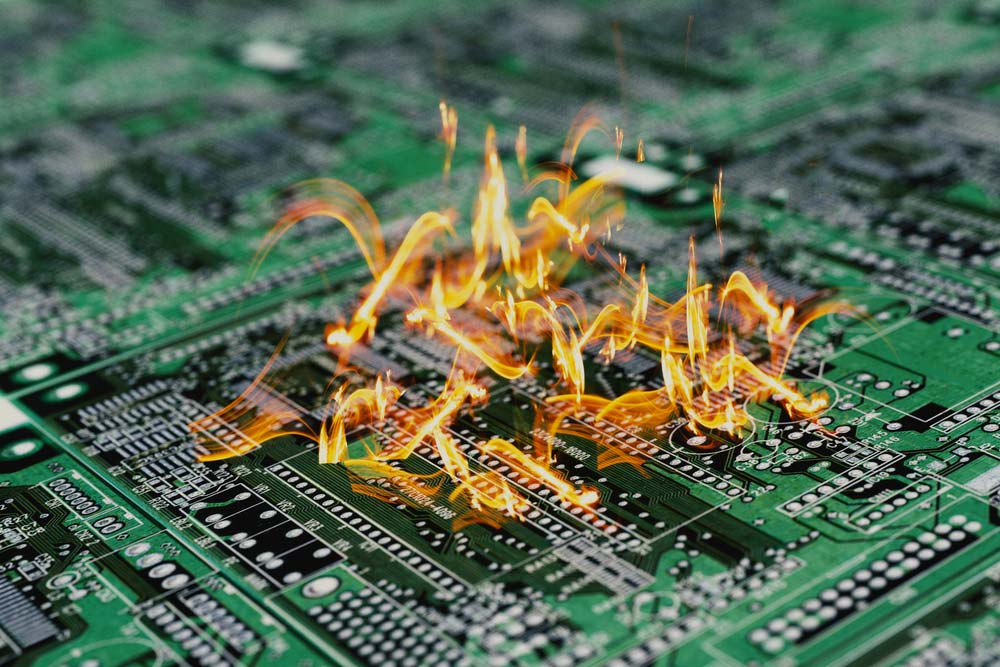
A PCB is on fire due to short-circuiting.
Crackling
The board can also emit crackling noises on contact or when you move it, caused by the copper traces that peel from the dielectric and move around the hollow space.
Corrosion
Corrosion can also occur when the board delaminates, and it can occur on the copper traces, the board material, or both. You will notice some spots on the surface where it should only be the solder mask’s color.
A close-up image of a corroded PCB
Effects and Consequences of PCB Delamination
Electrical Performance Issues
Delamination can peel the copper traces from the dielectric, which can cause noise, crosstalk, impedance variations, and signal reflections that downgrade the board’s electrical performance.
Heat Dissipation Issues
Air is not as good of a conductor of heat as FR4 and other board materials. These air gaps due to delamination create regions with thermal resistance that can stress active components on the board that generate a lot of heat.
High Chances of Failure
Besides electrical and heat issues, delamination weakens the PCB’s physical structure, making it vulnerable to vibrations and mechanical stress.
Reduced Lifespan
Combining a weakened structure, heat issues, and electrical problems reduces the printed circuit board’s reliability and lifespan.
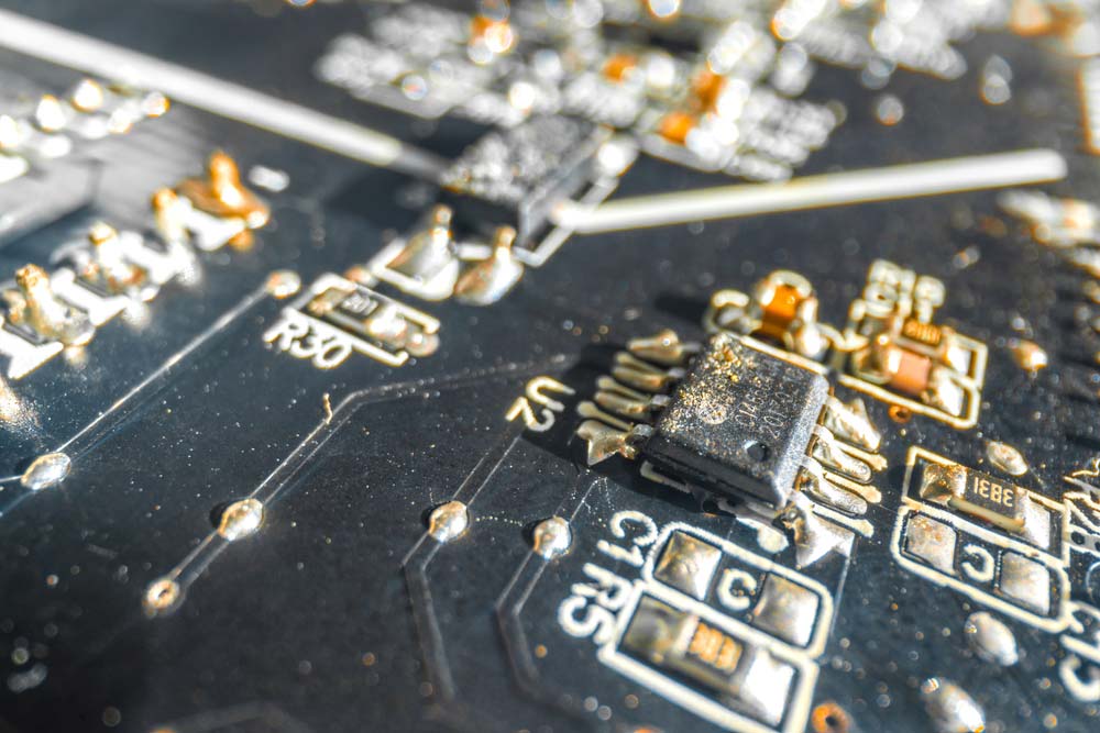
Repair and Rework Difficulties
Delamination makes it difficult to create proper electrical connections, such as reliable solder joints when handling repairs. You might have to remove the delaminated sections before doing these rework tasks.
Cracked solder joints on a PCB.
Higher Manufacturing Costs
Since you must rework or scrap the board once you’ve discovered this error, you’ll have a big loss to deal with to fix the issue. Even if the product passes the manufacturing process undetected, the consumer will encounter reliability issues that will damage your reputation and increase warranty claims.
Impaired Troubleshooting and Testing
Delamination can also interfere with the PCB troubleshooting and testing processes due to the electrical issues that can arise. Finding the root cause of this issue can be challenging, as well, which means longer downtimes.
Preventive Measures and Mitigation Techniques
Optimize the Design
Ensure you implement trace routing with the proper spacing and without sharp angles. Incorporate thermal management into the design, using things like thermal relief pads and heat sinks.
Pick the Best Material
Ensure this material meets the required PCB specifications, such as thermal cycling, mechanical strength, and low moisture absorption.
PCBs with an FR4 fiberglass base substrate.
Optimize Manufacturing
Control the lamination process during fabrication by preparing the surfaces and maintaining the proper pressure, temperature, and time. Extend this optimization to assembly by using the appropriate soldering profiles and techniques.
Implement Inspection and Quality Control Methods
Visual inspections, AOI, and reliability tests should be standard to ensure the board meets the performance and durability requirements.

Checking an electronic printed circuit board for damages.
Analyze Failures and Implement Corrective Actions
It is important to conduct a failure analysis to identify the root cause of the PCB swelling and fix it permanently. While at it, document the lessons you’ve learned when rectifying this issue to create a knowledge base to help you prevent or quickly fix delamination issues.
How To Prevent PCB Delamination
It is possible to prevent measling and delamination in the PCB manufacturing process by pre-baking the PCB base layers before fabrication and assembly. This step should evaporate all the moisture content.
Also, ensuring resin controls and running the reflow soldering process at the right temperature can prevent delamination.
Circuit board laminates tend to absorb moisture under improper humid storage conditions because the base materials are hygroscopic. So, you can prevent delamination by storing the board in dry places. Additionally, you must ensure the quality of the oxide layer in the board's inner layers is top-notch.
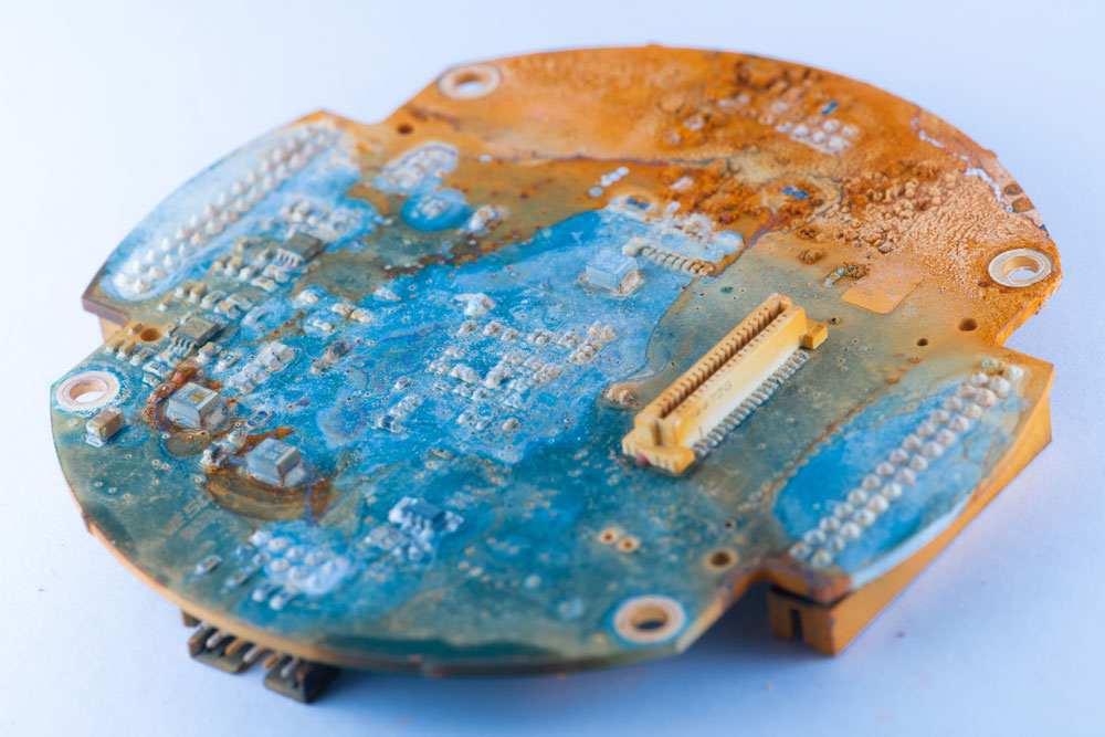
A water-damaged PCB
There's not much you can do as a designer to prevent this issue. Most of the responsibility falls in the hands of the manufacturer and assembler. So you need to employ the services of a high-quality PCB manufacturer. OurPCB has the required technical expertise & experience and high-quality machines to deliver delamination-free PCBs for your project.
Delamination Measurement Tests
Manufacturers usually use the time to delamination test for testing the base material performance. This time test measures how long the copper and resin or resin and reinforcement takes to separate/delaminate.
The test uses TMA (Thermomechanical Analyzer) equipment to elevate the temperature of a sample PCB to a specified level and then measure how long it takes for failure to occur.
Typical temperatures used for these tests are 260°C and 280°C, with the former considered more accurate and relevant in lead-free assemblies. The glass transition temperature plays a vital role in this test. Most low-Tg FR-4 materials exhibit higher times to delaminate than high-Tg FR-4 materials.
An FR-4 material PCB
Delamination Repair Steps
You can implement these repair steps to rectify a delamination problem. But first, you need the following items.
- Abrasives, ball mills, cutting tools
- Circuit bond epoxy
- Microscope
- Micro drill system
- Mixing picks
- Syringes
- Oven
- Wipes
Steps
- Clean the blister surface using wipes.
- Drill at least two holes into the delamination blister using the ball mill and micro drill. The holes should be opposite each other and around the blister's perimeter. Also, they should be clear of any components or circuitry. Brush off the loose material after drilling.
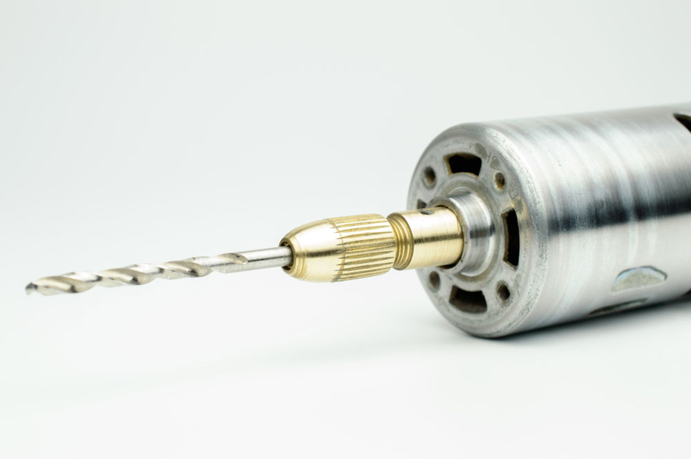
An electric micro drill for drilling PCBs
- Caution: Don't drill too deep to expose the inner planes or circuits. And keep in mind abrasive operations can generate static charges.
- Bake the circuit board in the oven to eliminate any moisture content. Don't let it cool before injecting the epoxy because moisture might condense and get trapped inside again.
- Caution: Some electronic components are sensitive to high temperatures. Don't take the heat too high.
- Pour the epoxy into the cartridge, then inject it into one of the drilled holes. The heat in the PCB should help distribute the epoxy, drawing it into the void area to fill the space.
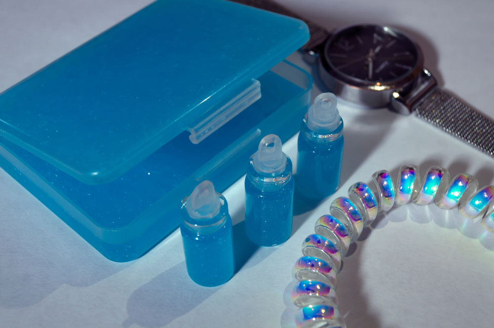
Blue epoxy resin bottles
- Apply light pressure on the board if the blister does not get filled. Begin at the fill hole and proceed to the vent hole slowly. Alternatively, you can apply a vacuum to the vent hole to pull the epoxy and fill the void.
- Cure the epoxy at room temperature for 24 hours or at 74°C (165°F) for one hour.
- Scrape off any excess epoxy using a scraper or knife. Apply a thin coat if required to seal the scrapped areas.
Evaluation
After drying, do a visual examination to check the color and texture. Also, do electrical tests on conductors around the repaired area to see if everything works.
Wrap Up
In summary, poor manufacturing processes are the leading causes of PCB delamination. Although there is a way to repair the issue, it is better to prevent it before it occurs. So look for high-quality fabricators like OurPCB to build you the boards for your project. Contact us with your layout files, and we'll give you a free quote before getting to work.
Special Offer: Get $100 off your order!
Email [email protected] to get started!