High-density interconnect circuit boards incorporate several technologies, such as resin-plugged vias, to handle the higher circuit density than traditional PCBs. These resin plug hole HDI PCBs is critical in developing compact, multi-layer circuit boards for tiny, complex electrical & electronics.Let's look at how to make these structures and their significance in the PCB manufacturing industry. Read on to learn more!
Contents
- What Is a Resin Plug Hole?
- Resin Plug Hole History
- Why Resin Plugged Holes?
- Types of Via-in-Pad Plugging
- Traditional Via-in-Pad Plugging
- Vacuum Plugging Resin Plugging
- Vacuum Adhesive Resin Plugging
- Resin Plug Hole HDI PCB Production Process
- Inner Layer Grinding Process
- Inner Layer Non-Grinding Process
- Through-Hole Resin Plugging Process
- Via-in-Pad Filling Process
- Copper Paste Plug Hole with an Electroplated Copper Cap
- Resin Plug Hole with an Electroplated Copper Cap
- Why Plug Via-in-Pads in HDI PCBs?
- Functions of PCB Resin Plug Holes
- Applications of Resin Plug Holes in HDI PCBs
- Wrap Up
What Is a Resin Plug Hole?
As the name suggests, a resin plug hole is a via hole plugged with resin material to enhance the circuit board's reliability by reducing the possibility of trapping liquid or air inside.This manufacturing technique gives a high yield (pass rate) when assembling high-density interconnect circuit boards.
Resin Plug Hole History
As electronic chips advanced through the years, PCBs needed to keep up with their advancements because they provided the circuitry to power and run the processors.Initially, the PCB industry standard used green oil plugging to fill vias to keep moisture and air out. If left open, the air or moisture would expand rapidly when the boards go into ovens for SMT assembly, causing the layers to unravel or pop up.But green oil plug holes affected PCB quality because they shrunk after fixing. Also, bubbles could appear in the hole. Via holes needed a better filling material to create a flatter surface for component mounting.A Japanese company solved the problem of air into the via-hole caused by green plug holes by inventing a resin suitable for via-hole filling.However, the technology at the time wasn't as advanced as it is now, meaning the resin did not get widespread adoption. Currently, the resin has multiple applications in the modern consumer electronics world, especially when dealing with the BGA chip mounting technique.
A BGA chip and pad on a PCB with via-in-pads
Why Resin Plugged Holes?
Traditional BGAs can have via-hole connections to the back between pads and a different pad connected to the surface for wiring. However, this fan-out design is not feasible for dense BGA connections in modern chips because the balls are too close to each other.So, as the designs became more compact and complex, the via hole could not go out of the pad's location. Manufacturers had to place pads for wiring directly above the vias.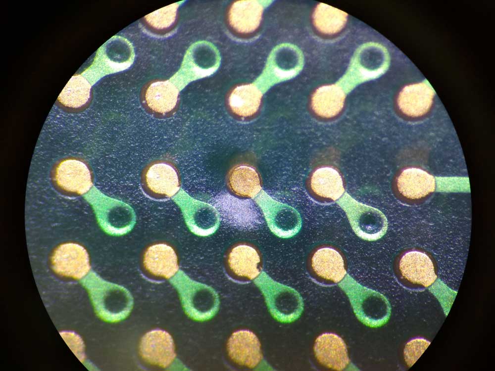
PCB pads with offset vias
This design introduced the popular term known as via-in-pad. The via-in-pad is the structure, but the manufacturing process is known as POFV (Plated-On Filled Via).
Types of Via-in-Pad Plugging
There are three different via-in-pad plugging types that either use conductive materials (silver or copper paste) or non-conductive resins to fill the hole.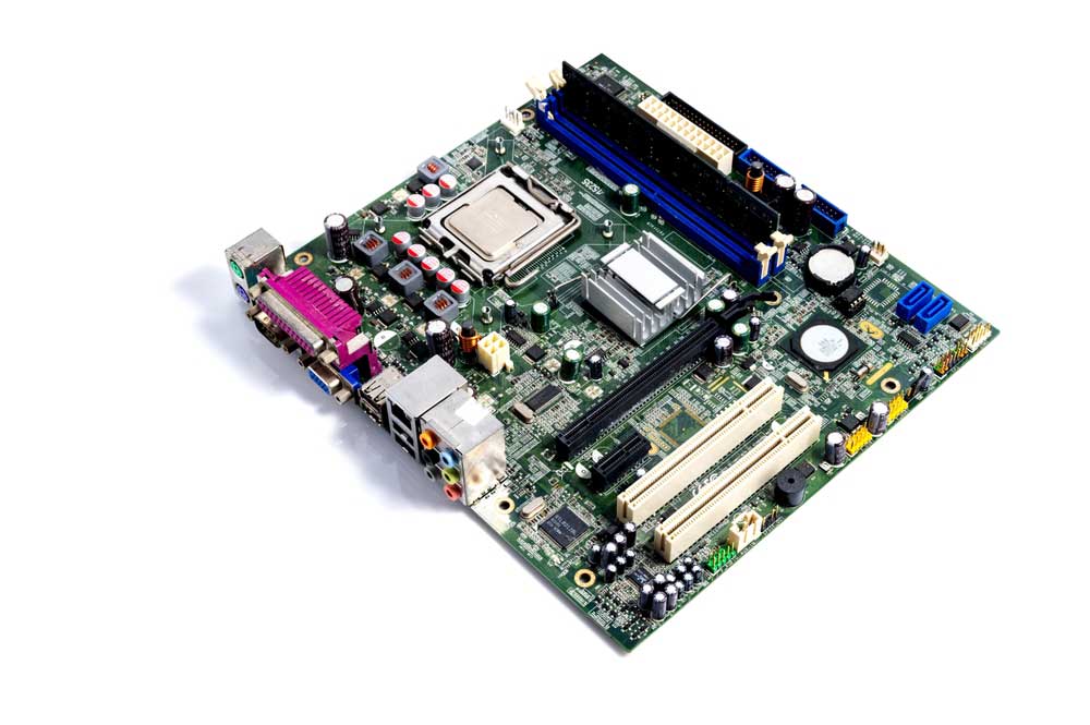
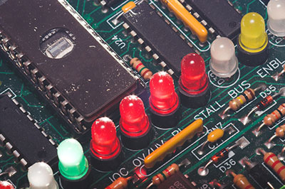
A dense modern computer PCB (motherboard)
Traditional Via-in-Pad Plugging
This process uses a permanent resin plugging ink as the plugging material. Also, it uses screen printing, aluminum stencil, and a special resin scraper as the plugging equipment.However, this type is not ideal for HDI PCBs because the hole plugs can be unstable and produce air bubbles.
Vacuum Plugging Resin Plugging
Vacuum plugging resin plugging is similar to the process above, except that hole filling occurs in a vacuum. So, it makes a more stable plug because it has zero or few air bubbles. And you'll need a vacuum plugging machine for this process, which is quite costly.
Vacuum Adhesive Resin Plugging
This resin plug technology requires a vacuum laminator, plus a PP film, aluminum sheet, release film, or copper foil as the materials. It creates a stable plug with zero bubbles or cracks.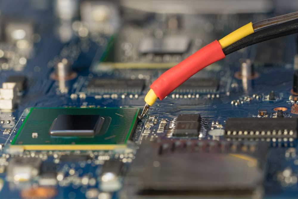
BGA chip soldering on a soldering station
Resin Plug Hole HDI PCB Production Process
Regardless of the via-in-pad plugging type you use, the plug-hole production process in HDI PCBs requires these steps.
- Cutting
- Via-in-Pad drilling
- VIP immersion copper and electroplating
- Via-in-Pad resin plugging into the hole
- Baking
- Grinding using a grinding plate
- Copper plating or plated-through hole
- Outer layer pattern
- Anti welding
- Surface treatment
- Molding
- Electrical testing
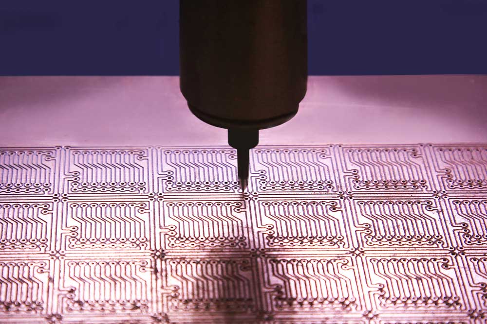
A drillbit drilling holes through a PCB for mounting chips
However, inner layer resin plugs require different steps categorized into grinding and non-grinding processes.
Inner Layer Grinding Process
This procedure requires the following steps.
- Cutting
- Buried hole inner layer pattern
- Automated Optical Inspection
- Pressing
- Drilling
- Electroplating
- Resin plugging
- Baking
- Grinding
- Inner layer lining
- Browning
- Pressing
- Drilling (laser or mechanical)
- Electroplating
- Solderproof surface treatment
- Electrical tests
Inner Layer Non-Grinding Process
As the name suggests, this process eliminates the grinding section, resulting in the following steps.
- Cutting
- Buried hole inner layer pattern
- Automated Optical Inspection
- Pressing
- Drilling
- Electroplating
- Inner layer lining
- Browning Treatment
- Resin plugging
- Flattening
- Baking
- Pressing
- Laser or mechanical drilling
- Electroplating
- Surface treatment
- Forming
- Electrical testing
Through-Hole Resin Plugging Process
Through-holes undergo these steps for resin plug-hole creation.
- Cutting
- Drilling
- Electroplating/PTH
- Resin plugging
- Baking
- Grinding
- Outer layer patterning
- Surface mounting
- Surface treatment
- Forming
- Electrical performance testing
Chip mounting in through holes on a PCB
Special Offer: Get $100 off your order!
Email [email protected] to get started!
Via-in-Pad Filling Process
Here's how to fill the pad with conductive or nonconductive plug materials.
Copper Paste Plug Hole with an Electroplated Copper Cap
Vias have conductive metal-plated sides. So, filling them with conductive pastes, such as copper or silver pastes, is recommended for situations requiring quick heat dissipation.Therefore, this process is ideal for GND thermal relief pads under Quad-Flat No-leads packages (QFNs). It involves filling the hole with the conductive paste and then covering the top to seal it using immersion or electroplated copper.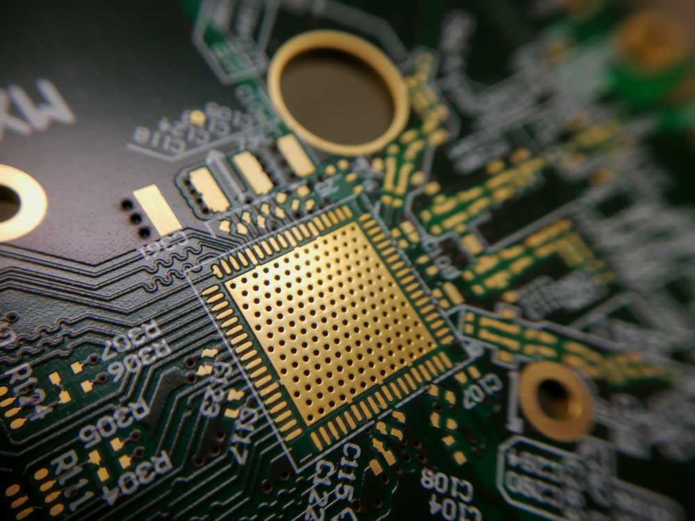
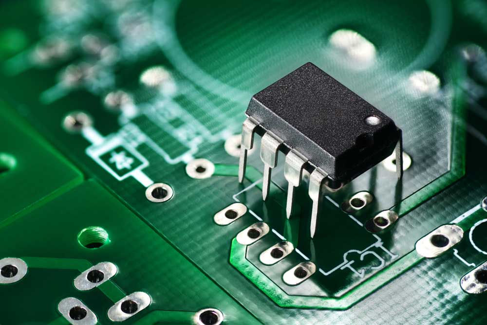
A QFN thermal pad on a PCB with conductive-material-filled vias
Resin Plug Hole with an Electroplated Copper Cap
This process involves filling the hole with epoxy resin and electroplating copper above the surface to seal the material. It creates a smooth, non-sinking outer hole surface with zero perforations that allow tin leakage inside when soldering.
Why Plug Via-in-Pads in HDI PCBs?
Plugging pads in HDI PCBs is necessary because it has the following benefits.
- Prevents residual flux from filling the holes, causing corrosion
- Enables faster heat dissipation in thermal vias via thermal relief pads
- Keeps surface waste from getting into the holes
- Prevents short-circuiting caused by tin flowing into the hole (when soldering BGAs and other fine-pitch devices)
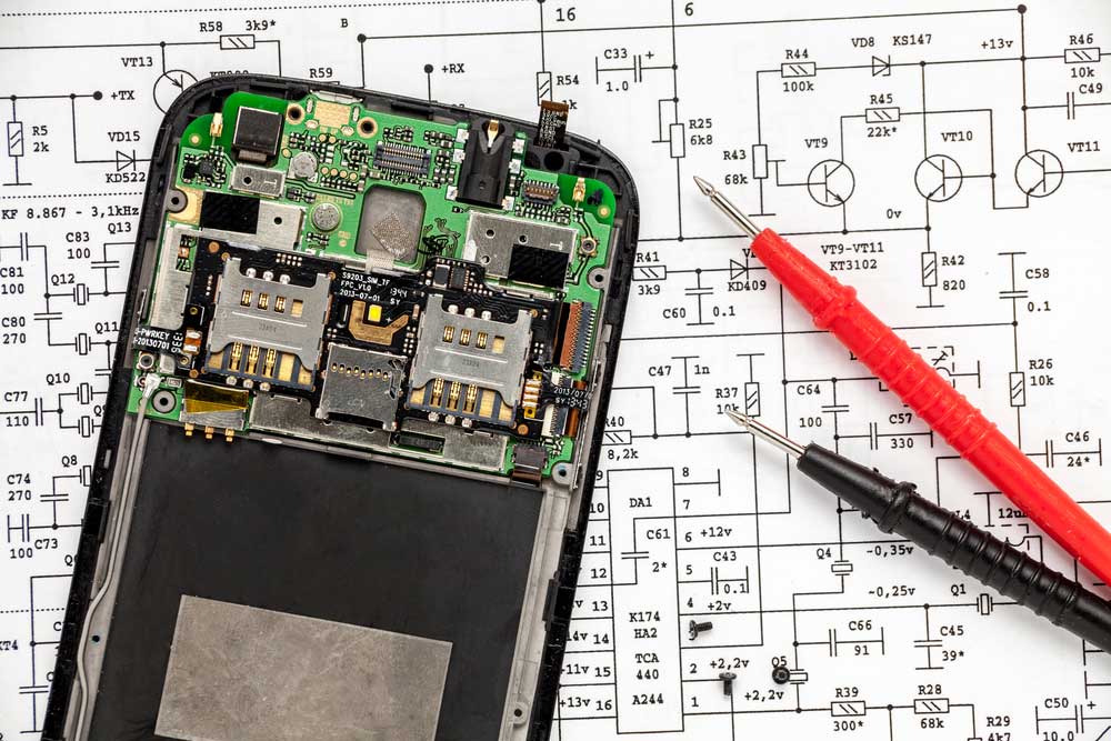
An HDI dual-sim smartphone PCB undergoing repairs
Functions of PCB Resin Plug Holes
- Eliminates the typical surface sinking issues that result from lamination flow glue underfilling.
- Reduces hole spacing (pitch)
- Enhances the reliability and electronic performance of electronic products/appliances
- Effectively utilizes the 3D space between inter-layer connections
- Solves the wires and wiring problems
Applications of Resin Plug Holes in HDI PCBs
Resin plug holes are typical in high-density circuit boards to help them meet the thin dielectric layer design requirements. You'll also find them in HDI boards with buried vias to thin the inner dielectric layer thickness.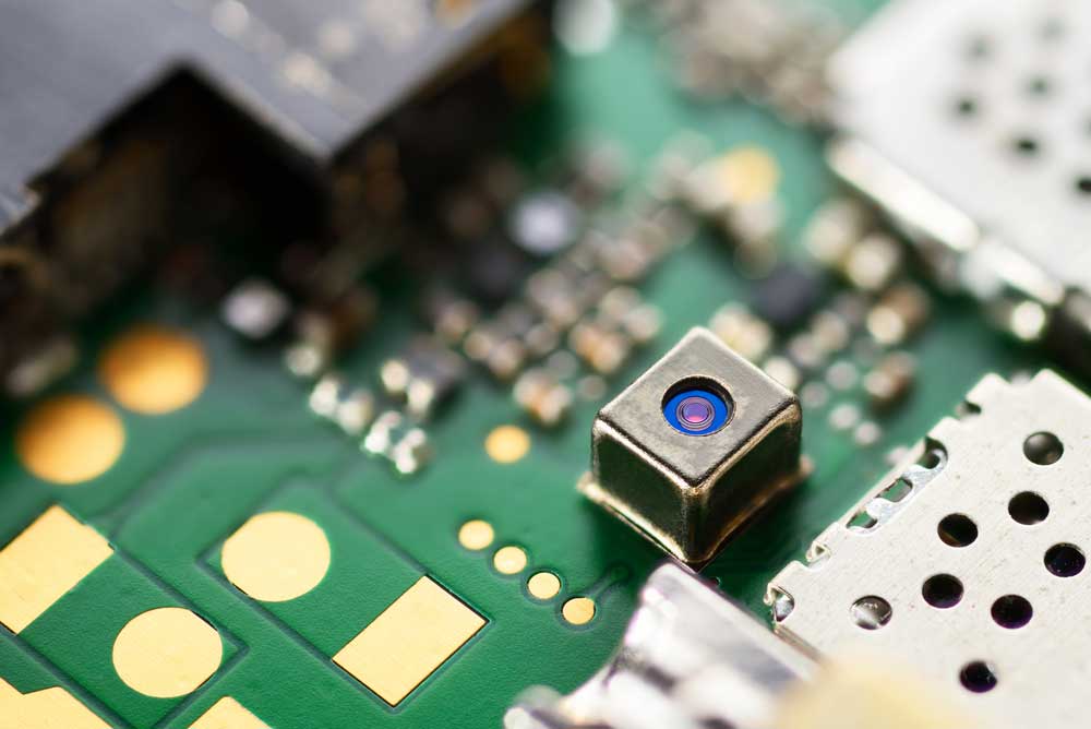
A phone PCB with an SMD camera mounted on board
Lastly, the resin plug holes are critical in blind microvias with dielectric thicknesses greater than 0.5mm. In these situations, you cannot use hole-filling glue to fill the blind hole fully when pressing.So, it would be best to use HDI plug holes (for complete hole filling) to avoid having zero copper on the pad after pressing.
Wrap Up
Resin-plugged holes are critical in fabricating HDI PCBs because they make their structures and electrical properties more reliable.Creating them is challenging, but fabricators continuously enhance their PCB manufacturing process to reduce the scrap rate after board production and assembly.That includes our manufacturing team, which can make reliable, high-quality HDI PCBs for your project. Contact us with your specifications, and we'll deliver your PCB shortly.
Special Offer: Get $100 off your order!
Email [email protected] to get started!