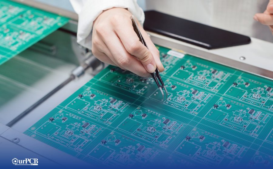
Printed circuit boards exit the production lines as non-functional bare boards because they don’t have signal-controlling components. For this reason, PCB soldering is critical in PCBA production because it enables you to create electrical and mechanical connections between the board and these components.
Soldering plays two general roles when assembling PCBs. The first is to join through-hole components to plated-through holes, and the second is to attach surface-mount components to solder pads on the board’s surface. Below, we look at this PCB assembly process in detail, including the soldering types, tools, materials, steps, and common mistakes.
Contents
- What is Soldering?
- What are the Different Types of Soldering in PCBs?
- Soft Soldering
- Hard Silver Soldering
- Braze Soldering
- Wave Soldering
- Reflow Soldering
- Tools and Materials Needed to Solder a PCB
- Soldering Iron
- Solder
- Soldering Stand
- Flux
- Desoldering Tools
- Wire Cutters and Strippers
- Heat-Resistant Tweezers
- Safety Equipment
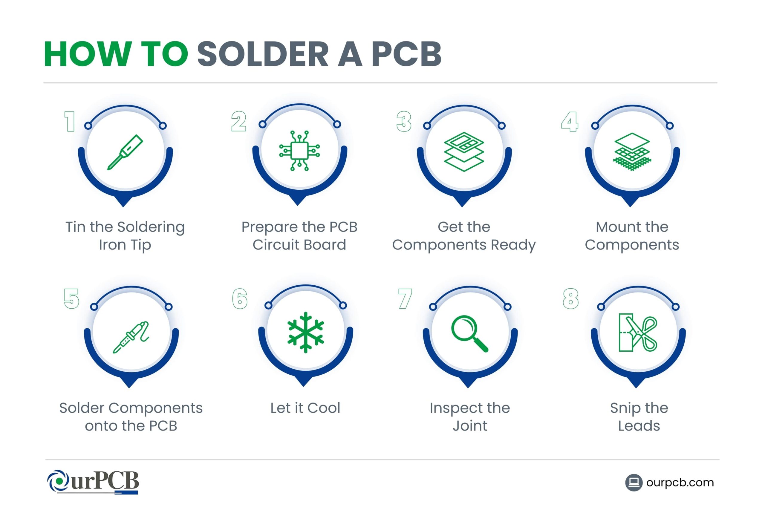
- How to Solder a PCB
- Tin the Soldering Iron Tip
- Prepare the PCB Circuit Board
- Get the Components Ready
- Mount the Components
- Solder Components onto the PCB
- Let it Cool
- Inspect the Joint
- Snip the Leads
- Common Soldering Mistakes to Avoid
- Tips to Solder a PCB Circuit Board
- Keep the Iron Tip Clean
- Use Heatsinks
- Control Solder Flow
- Solder Small Parts First
- Install Sensitive Components Last
- Use Solder Wicks for Cleaning
- PCB Soldering FAQs
- What Temperature Should You Use for Soldering?
- Why is it Important to Clean the PCB After Soldering?
- Can PCBs Be Soldered Directly Together to Make an Adapter?
- Why is Your Soldering Iron Leaving Black Residue on the Board?
What is Soldering?
Soldering is a welding technique that involves joining metal components using molten metal, which is known as solder. The resulting metal joint allows electrical current to flow across the board’s circuit and the joined part.
The process requires flux to clean and prepare the metal surfaces before applying molten solder – a tin or lead metal alloy.
What are the Different Types of Soldering in PCBs?
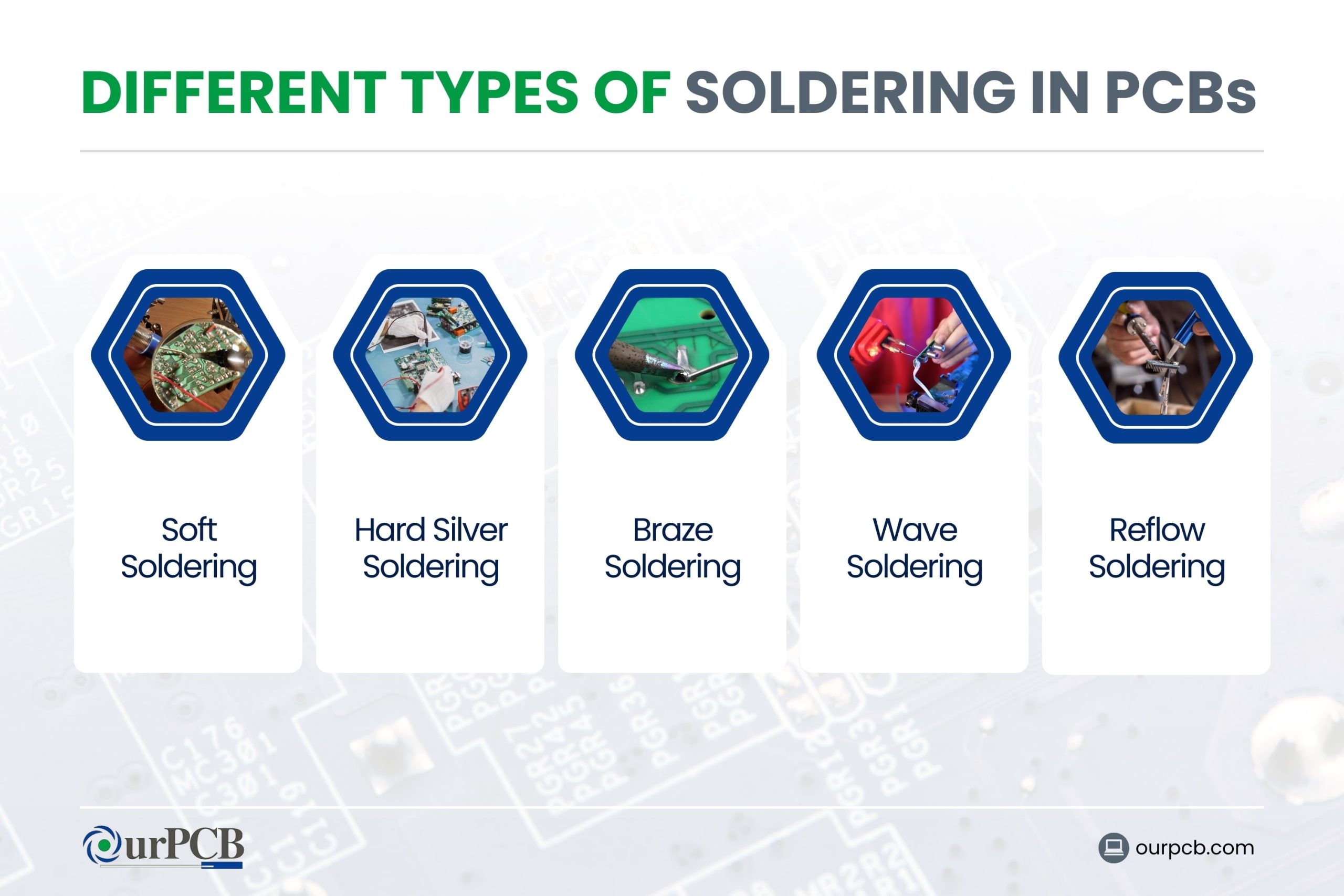
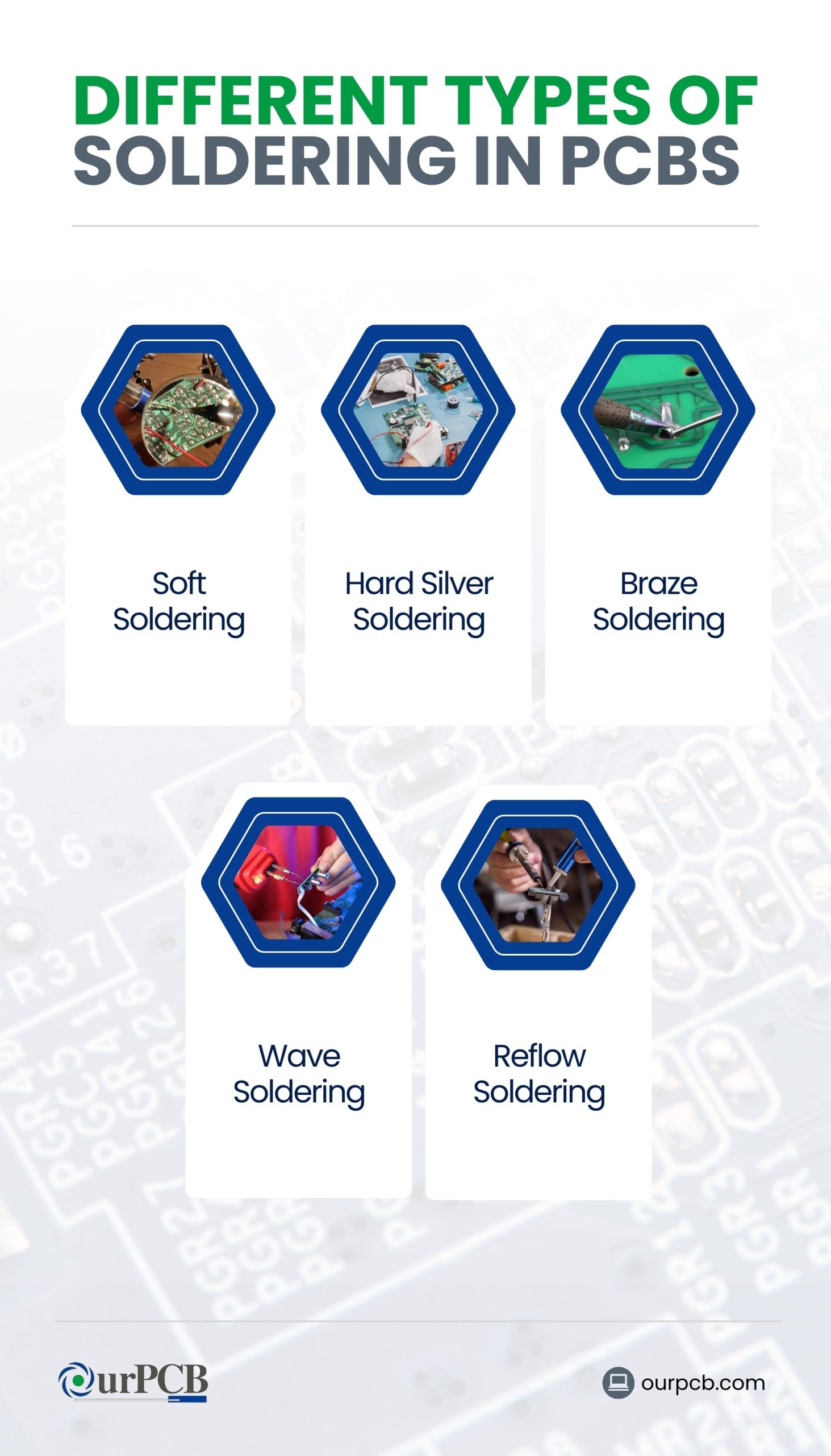
Soft Soldering
Soft soldering is often used to attach small electronic components to PCBs with tin-lead alloys as the filler materials. Tin-lead alloys melt at 400° C (752° F) max, so you can use a soldering iron to melt the metal.
Hard Silver Soldering
As the name suggests, this soldering type requires a silver alloy, such as cadmium-silver, as the filler material. Hard silver alloys contain as much as 80% silver, which raises the material’s melting point to 740° C (1,370° F). You’ll need a carbon-arc torch or flame to reach these temperatures.
Silver is usually absorbed by the surrounding metal, creating a joint that is stronger than the metals being joined. However, this filler material runs freely and will not fill gaps, so the two metal ends must be flush.
Braze Soldering
Brazing is similar to hard silver soldering because it requires high temperatures to melt the solder. But in brazing, the solder wire or rod contacts the joint while being heated. With hard silver soldering, the silver pieces are positioned on the joint before applying heat.
Wave Soldering
is a bulk soldering process used to weld through-hole components to PCBs. The boards travel on a conveyor above a pan of molten solder, where a pump creates an upward flow of the molten metal to create a standing wave. This wave contacts the PCB underside, soldering the pins of the inserted components to the plated holes.
Reflow Soldering
Bulk soldering of surface-mount components requires reflow soldering, a process that begins with solder paste printing using a stencil, component placement using a pick-and-place machine, and then reflow soldering in an oven.
Special Offer: Get $100 off your order!
Email [email protected] to get started!
Tools and Materials Needed to Solder a PCB
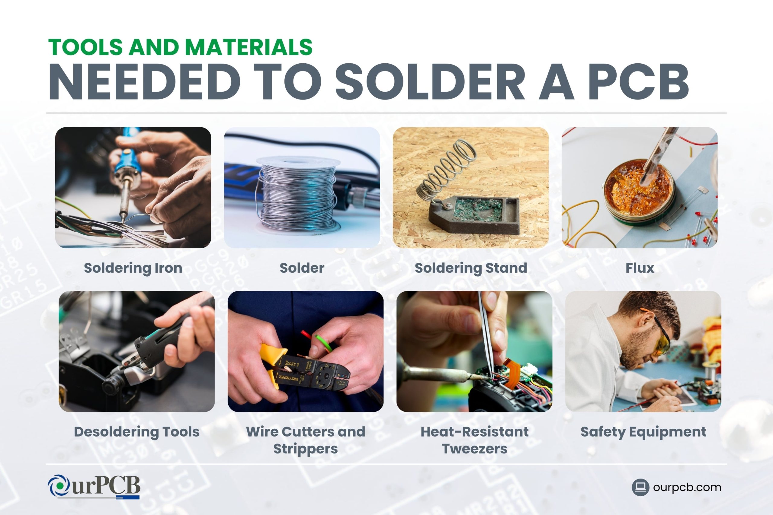
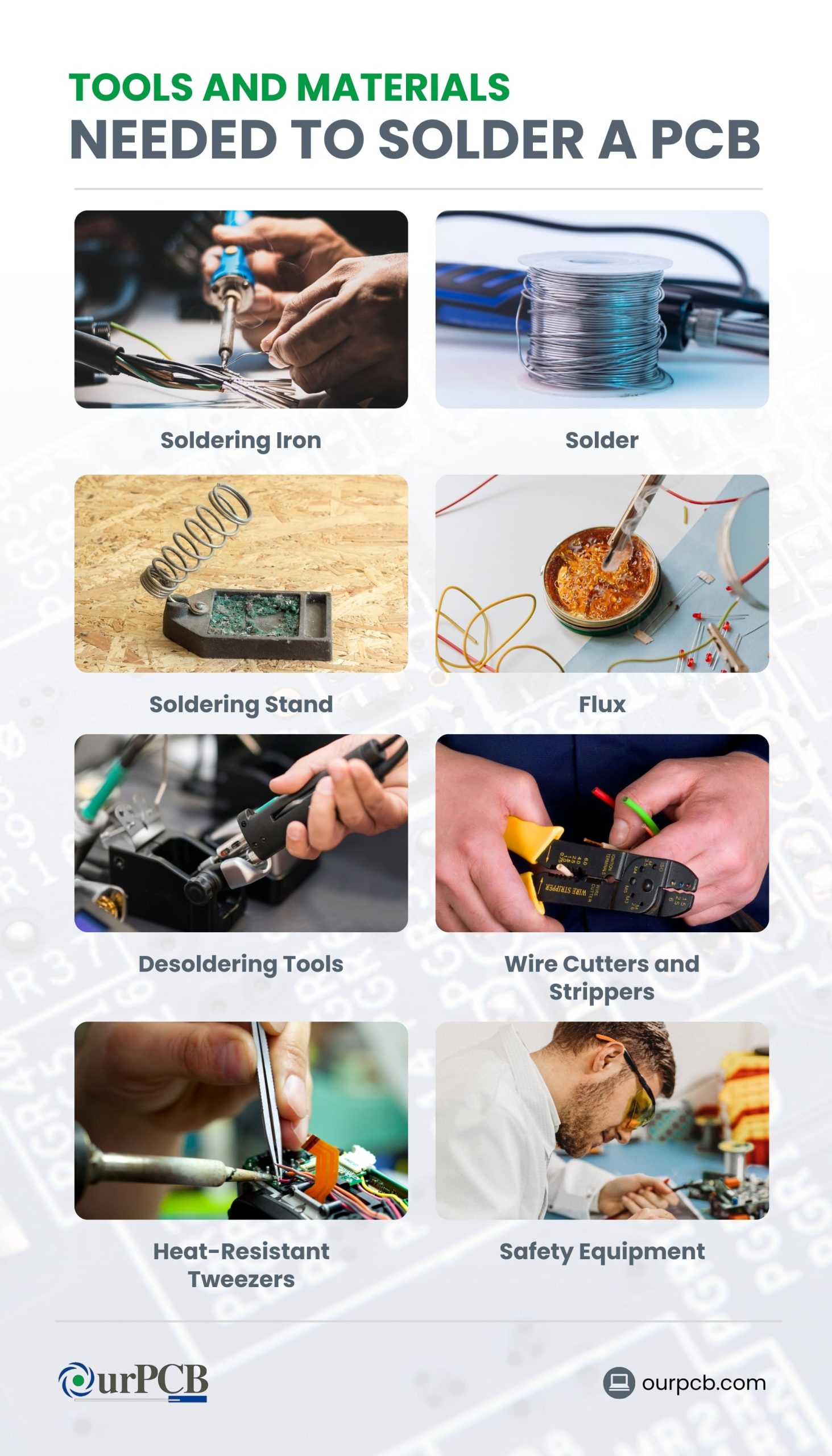
Soldering Iron
generate the required heat to melt the solder and weld the parts. They come in different types, such as:
- Corded
- Cordless
- Adjustable temperature (temperature-controlled)
- Hot knife
- Tweezer
The choice between these types depends on various factors. For instance, a cordless iron is suitable if you don’t have power because it runs on batteries or butane. If soldering tiny 2-terminal SMT devices, tweezers would be more appropriate.
Temperature-controlled soldering irons can be standalone units or be part of a complete soldering station, and they deliver precise heating to suit different manual soldering tasks.
Solder
Solder can either be in the form of a solid wire or paste. The former is ideal for soldering through-hole components, and the latter for SMDs. Solder wires range from 0.015 to 0.062 inches (0.381 to 1.57 mm) in diameter, and you can also use the thinner ones in this range for SMD soldering.
Either variety can be lead-based or lead-free, with the latter being recommended because lead is harmful to the environment and highly toxic to the human body. Some directives, such as RoHS, ban lead use in electronics due to its hazardous nature.
Soldering Stand
Since the iron’s tip will be hot when soldering, you need a stand to suspend it above the work surface away from flammable parts, sensitive components, or the workstation surface material. But a stand is not necessary if you have a soldering station.
Flux
Flux is an acidic chemical/purifying agent that has three functions:
- Cleans the component leads and solder pads to eliminate rust or oxidation
- Seals the solder joint to prevent air pockets inside that can cause rusting or oxidation later
- Enhances the wetting ability of the solder to create strong joints
There’s no need to apply this chemical when using solder paste because it is suspended in flux paste. Some solder wire varieties have a flux core to avoid external application, but it is recommended to apply flux, as the flux in the wire might be insufficient.
Desoldering Tools
If you make mistakes when soldering, desoldering tools like solder wicks and suckers (desoldering pumps) will be handy.
Wire Cutters and Strippers
If you’re soldering wires to PCB pads, you’ll need wire cutters to cut the cables to size and strippers to prepare the leads by exposing the metal.
Heat-Resistant Tweezers
Components can get hot when soldering or desoldering, so heat-resistant tweezers will help you grab tiny parts or wires safely.
Safety Equipment
Dealing with molten metal has its safety risks, so it is necessary to have safety equipment like protective eyewear, heat-resistant gloves, and a fume extractor.
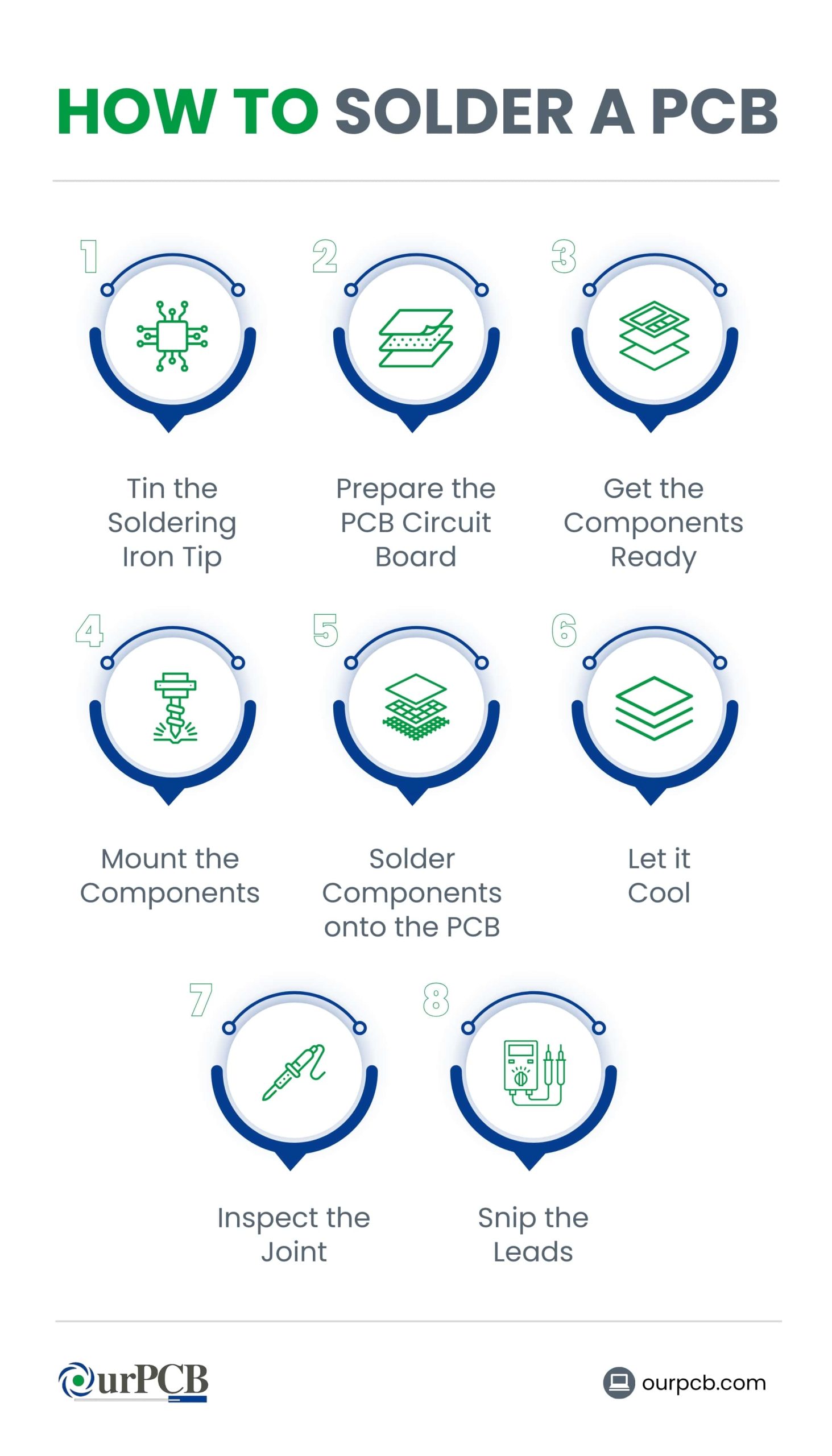
How to Solder a PCB
-
Tin the Soldering Iron Tip
Once the iron is hot, wipe it with a wet sponge, then tin it. Solder iron tip tinning refers to dipping a hot tip in solder paste or touching the wire to it when hot. This step creates a protective solder (tin) coat above the tip that reduces wear and improves heat transfer to the soldering surface.
-
Prepare the PCB Circuit Board
Clean the soldering surface using an acetone cleaner or industrial cleaning wipe to remove dust and debris. We recommend using compressed air afterward to dry the surface quickly and remove small particles.
-
Get the Components Ready
Select the components to solder first, which should be the small components. Always solder the large parts last because they can weigh down the PCB. Separate these parts by size to know the order in which to mount and solder them.
-
Mount the Components
Insert the component leads into the through holes and bend them on the other side outward at a 45° angle. Bending the leads allows you to hold the component still when soldering and connect better to the pad.
-
Solder Components onto the PCB
Turn on the tinned soldering iron to around 400° C and touch the tip to the joint to warm the pad and component lead. After 3 to 4 seconds, touch the solder to the hot joint, which should be hot enough to melt the wire. Let the solder wet the entire joint, and ensure you avoid touching the solder wire directly to the iron’s tip.
-
Let it Cool
Remove the iron from the joint and give the solder time to cool. Ensure you keep the PCB surface flat and still as the metal solidifies.
-
Inspect the Joint
Once solidified, inspect the joint to ensure it has a smooth, shiny cone.
-
Snip the Leads
Trim the extra wire from the component lead, then clean excess flux from the joint.
Common Soldering Mistakes to Avoid
| Common Soldering Mistake | Mistake Explained | How to Fix |
| Using Too Much Solder | Applying too much solder forms a round, bulging joint that resembles a bubble. | Remove this excess solder using a desoldering pump or solder wick. |
| Solder Starved | If the solder is insufficient, the joint will be weak and can break easily under minimal stress, resulting in an open circuit. | Let the solder continue flowing into the joint when soldering to fill the pad adequately. |
| Solder Bridges | Solder bridges are unintended solder connections between two pads that create short circuits on the PCB. | Use a soldering iron to heat the joint, then remove the excess solder using a desoldering pump or solder wick. |
| Cold Joints | These joints occur when the joint isn’t hot enough to make the solder melt and flow properly. | Reheat the joint adequately by extending the contact time or raising the iron’s temperature to the recommended level until the solder flows smoothly when touching the pad. |
| Disturbed Joints | If you move the joint before the solder cools and solidifies, it forms a disturbed joint. | Reheat the joint and let it cool undisturbed on a level surface. |
| Overheated Joints | Overheated joints appear whitish with charred marks and a distinct bulge. | Lower the iron’s temperature or contact it to the pad for a shorter period. |
| Insufficient Wetting | Proper wetting can only occur on a clean soldering surface. With insufficient wetting, the solder doesn’t flow properly on the surface. | Clean the solder pad using an acetone cleaner or industrial cleaning wipe, then use flux to remove oxidation and other impurities. |
| Lifted Pads | A solder pad can lift off the circuit board if excessively worked or overheated. | Repair the pad using a jumper wire or replace the mounted component. |
| Skips | Skips are termination points that don’t have any solder. | Apply solder using the steps explained above. |
| Webbing and Splashes | Excess solder can form splashes or web-like structures on the PCB that cause shorting. | Remove this excess solder using a desoldering pump or solder wick. |
| Tombstoning | This fault is common on SMDs, where one end or terminal lifts off the pad when soldering. | Reheat both joints, ensure they have enough solder, and apply enough pressure gently to hold the component down as the solder solidifies. |
| Stray Solder | Stray solder refers to tiny bits of tin that solidify unintentionally on the board’s surface after soldering. | Use tweezers or solder wicks with an iron to remove the metal. |
Tips to Solder a PCB Circuit Board
Keep the Iron Tip Clean
A dirty iron tip experiences faster corrosion, resulting in quick wear. Any buildup on this tip, including oxidation, will also affect the soldering process by delaying the heat transfer process and lengthening the soldering time.
Use Heatsinks
Heatsinks are necessary to protect sensitive components like transistors and ICs from heat stress and damage. Also, you should install a thermal mat or board to protect your work area from fires or tarnishing due to the high temperatures.
Control Solder Flow
Precise solder flow control reduces the risk of soldering defects like cold joints and solder bridges, which cause shorts.
Solder Small Parts First
Beginning with larger, heavier components can weigh down the board and make the surface sit unevenly. Therefore, the general rule of thumb is to start by soldering small components and finish with the large ones.
Install Sensitive Components Last
Sensitive components are susceptible to static, such as CMOS ICs and MOSFETs. If installed first, static charges generated when handling other parts can damage them.
Use Solder Wicks for Cleaning
A soldering wick is necessary in your work area to pick up excess solder that can short the circuit. Also known as a desoldering braid, this tool is critical for reworking parts of the circuit to rectify mistakes.
PCB Soldering FAQs
What Temperature Should You Use for Soldering?
The temperature used for soldering depends on the solder type. Leaded solder melts at lower temperatures than its lead-free counterpart, turning to liquid at around 315° C to 350° C (599° F to 662° F). Lead-free solder requires higher temperatures between 350° C and 400° C (662° F and 752° F) to melt.
Why is it Important to Clean the PCB After Soldering?
Cleaning is important because it removes the acidic flux residue, which can be corrosive or conductive, especially if the PCB has fine-pitch components.
Can PCBs Be Soldered Directly Together to Make an Adapter?
Yes, you can use castellations, which are plated half holes on the PCB edge, to solder circuit boards directly together without using additional components.
Why is Your Soldering Iron Leaving Black Residue on the Board?
A soldering iron can leave a black residue because of an oxidizing tip-plating, which forms iron oxide, a black compound. This residue could also be due to carbonized or burnt flux deposits.
Back to top: PCB Soldering
Special Offer: Get $100 off your order!
Email [email protected] to get started!