(PCBs) are among some of the most complicated components of any electrical device.
Many small things come together to create a properly functioning PCB. PCB copper weight is one of these many things that must be wholly understood and micromanaged when manufacturing PCBs.
Because it is such an intense conductor, copper is one of the most significant components of a PCB.
If you don't calculate and apply the weight of copper correctly, many things will go wrong.
It cannot be straightforward to measure and calculate PCB copper weight. There is also a lot of information about the PCB copper weight available. This article will put all this information together.
Contents
- 1、What is the PCB Copper Weight?
- Copper is an alloy
- 2、Design Considerations With Heavy Copper
- 3、PCB Copper Weight Specifications
- 1. Standard copper
- 2. Heavy copper
- 3. EXTREME copper
- 4、PCB Base Weight vs. Copper Plating Thickness
- 5、How is the Weight of the PCB Copper Finalized? - The Copper Weight Calculator
- 6、Heavy Copper and EXTREME Copper in PCB Design
- 6.1 How copper weight impacts PCB manufacturing
- 7、Conclusion
1、What is the PCB Copper Weight?
The significant building block of any PCB. As mentioned earlier, copper is a massive conductor. Creating a good PCB that works consistently without correctly measuring copper weight is nearly impossible.
It brings up the question: What exactly is PCB copper weight?
A specific set of calculations determines copper weight. It is then applied to the rest of the PCB and connected to everything else. The PCB is ready to be manufactured when the analyses are performed correctly.
It sounds simple enough, but specific things need to know about copper that contributes to copper weight calculations.
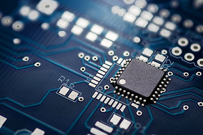
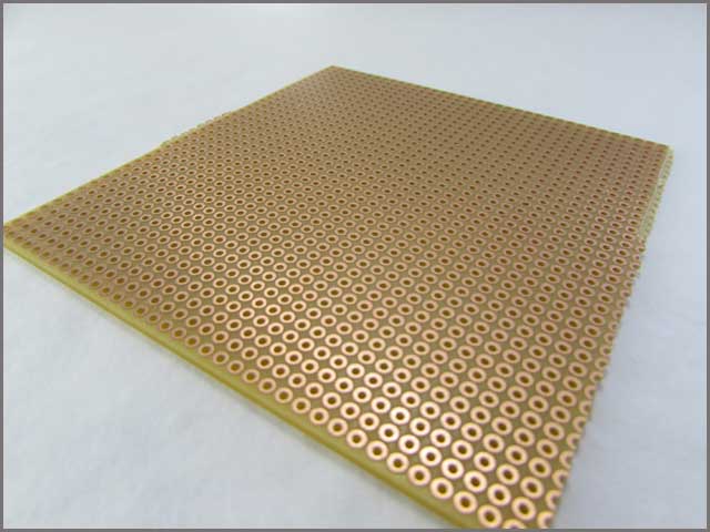 Image 1: PCB Copper Weight
Copper is an alloy
Like any metal, copper is an alloy. It is what makes it a conductor. Alloys come in many forms, but copper is the most common in constructing PCBs.
Alloys come in many forms, whether it is a bar, a sheet, or a tube. It is the first thing to consider before determining the weight of the PCB copper.
Knowing the grade and what form the copper takes are only two of several things that calculate the PCB copper weight itself. The rest pertains to physical measurements involving the copper itself.
One thing that needs to be mentioned is that these calculations and measurements must be perfect.
Failing to do this will not cause significant problems, but returning and remeasuring things will take a long time and be troublesome.
The worst-case scenario is applying the copper to the circuit board after making incorrect calculations. In this case, it would be tough to undo what has been done, if not impossible.
2、Design Considerations With Heavy Copper
In the previous section, we learned about the weight of PCB copper. This section will explore how heavy copper can be used to enhance the design of a PCB.
Copper thickness in ounces. Heavy copper can be as thick as 20 ounces per square foot. It makes it a popular option for many PCBs since most of today's electronics are much smaller than electronics in the past.
While other sizes of copper are still useable, heavy copper has become the most common and most popular.
Heavy copper allows for a lot more options in designing a PCB. Experts in PCB production and design have discovered ways to improve PCB looks because heavy copper is very versatile.
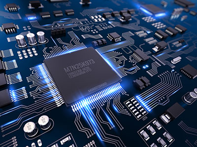
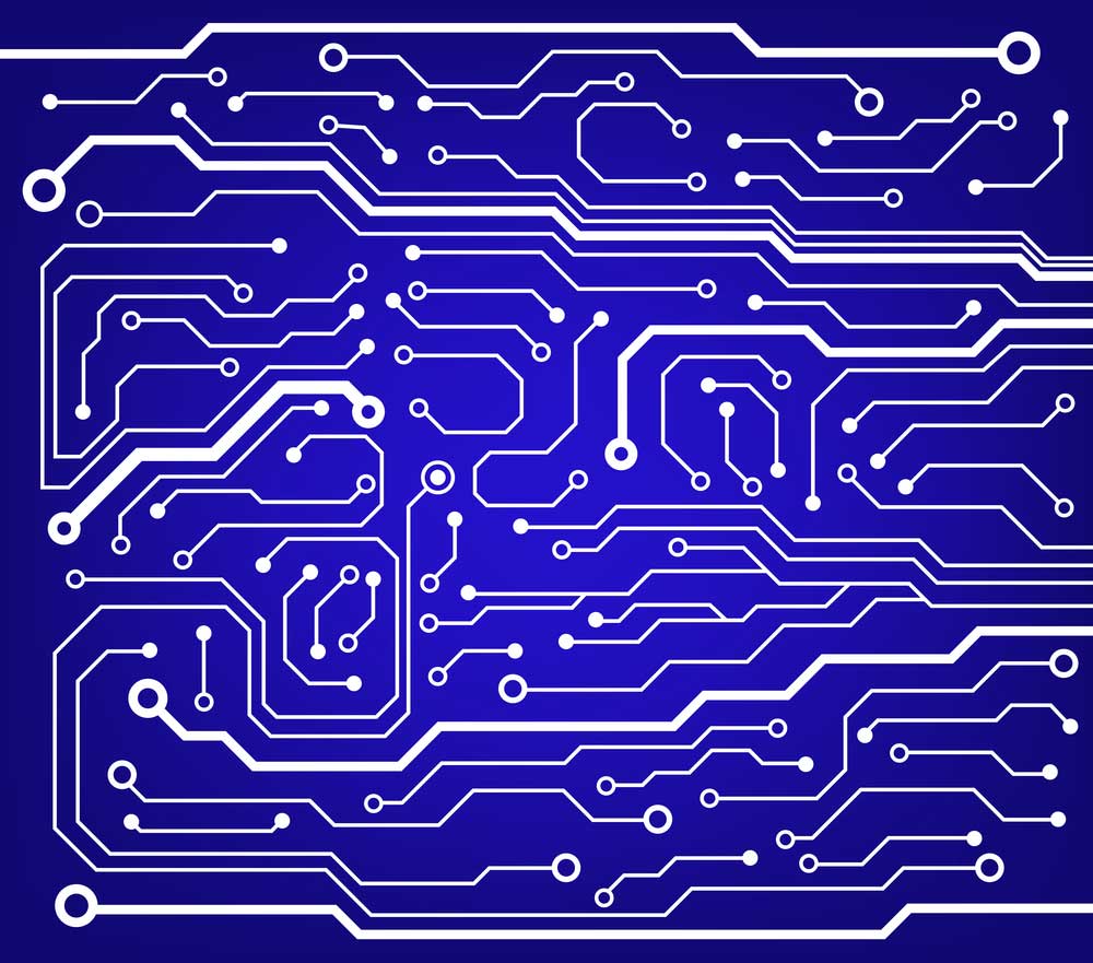
 Image 2: PCB Copper Weight
Another reason is that copper only accounts for a small amount of space on a circuit board in PCB production. Because of this, they are using the standard green rectangular board outline not necessary.
From this, it is now possible to create PCBs that function well and look a little more desirable than they used to.
Because of this, it is now possible to create artwork out of PCBs such as this:
Doing this is not as difficult as you would think. It takes a good knowledge of copper weights, measuring and weighing copper, and basic soldering techniques.
Special Offer: Get $100 off your order!
Email [email protected] to get started!
3、PCB Copper Weight Specifications
The previous section was about how heavy copper can be used to improve the aesthetics of a PCB. This section will describe the three specifications of copper weight.
There are three "weight classes" of copper. Each of these has its use in PCB manufacturing.
Copper thickness is measured in ounces per square foot. Because copper is such a strong conductor that yields predictable amps and mils, measuring it per square inch is unnecessary. It makes sure that other calculations are accurate.
1. Standard copper
Any copper plating of ¼ of an ounce per square foot to 4 ounces per square foot is considered standard.
This was the de facto industry standard for building almost any given PCB for a long time, as there was a shallow risk of failure when using it to plate a PCB.
Still using standard copper today, and in many cases, if a particular size of copper is not specified, many materials distributors will assume that the manufacturer desires 1.2 ounces per square foot of copper plating.
2. Heavy copper
Copper 5 to 19 ounces per square foot is considered heavy copper. Over the years, testers and designers have used heavy copper to experiment with their designs. As mentioned earlier, it is now possible to create a PCB with heavy copper, and in many cases, it is superior to standard copper.
For years, this was considered risky, as most believed copper was too strong a conductor to be plated onto a circuit board without terrible things happening.
Recently, this proved wrong, as it is still possible to lessen the amp value of the charge produced from heavy copper by exposing the copper before plating it onto a surface. What results in the ability to create customizable designs of copper plating onto a PCB?
3. EXTREME copper
It was not enough for some testers, as they decided to go further. What if it were possible to possess copper that was even thicker than heavy copper but could create lasting and powerful charges?
EXTREME copper is the result of this. The copper that is 20 to 200 ounces per square foot is considered EXTREME copper, and naysayers over the years have considered this unthinkable to plate into any PCB.
After all, even PCBs placed inside even the largest electronics only needed to possess heavy copper plates at most.
It was the case until the 2010s when testers discovered it possible to use EXTREME copper in a PCB, provided the charges they yielded were somewhat restricted.
These restrictions are made possible by performing a "Powerlink," which is achieved by placing at least two copper weights on the same PCB layer. While this is only possible on the outer layers, it proved it could plate EXTREME copper onto a PCB.
Now we know three kinds of copper weight classification. The next chapter will be about the copper plating process.
4、PCB Base Weight vs. Copper Plating Thickness
On its own, copper does not achieve anything as a conductor. It needs to be heated or cooled to certain levels to carry a charge in any PCB. The classification of PCB copper weights above describes base copper weights that are entirely unaltered.
Plating thickness is determined when copper is heated or cooled to certain levels. This chart shows a clear relationship between the unaltered copper weight, trace width, which pertains to a cross-section of copper, usually measured in millimeters (or "mils" for short), and current carrying capacity.
Some manufacturers make a mistake because they do not consider temperatures and traces when determining plating thickness. They will consider one thing but not the other.
This mistake occurs because, unlike many other operations that determine PCB copper weight, knowing trace width and temperatures is generally not part of calculations when finalizing PCB copper weight.
We explored the copper plating process. The calculation method of copper weight will be accurately displayed below.
5、How is the Weight of the PCB Copper Finalized? - The Copper Weight Calculator
Recall that copper is an alloy that requires a set of calculations to determine its final weight. Some of these methods were mentioned earlier, but these calculations will be explored now.
Before starting any copper weight calculation, you should know the difference between copper and copper alloy. While pure copper is an alloy in and of itself, there are some cases where it is combined with another alloy, such as nickel, to form a "copper alloy."
These have different grades than pure copper.
Both pure copper and copper alloy have a grade. The grade of pure copper starts with a "C," followed by a number. There are other grade families of copper, but when determining a PCB copper weight, pure copper and copper alloy are the most common forms of copper. Both of these have specific grades.
PCB Copper Weight
The grade of pure copper or copper alloy is something that you should know before ordering it, as the quality is usually listed on any given order form. Different grades of copper are used for other purposes, but C110 is the grade of copper used the most among PCB manufacturers.
The next thing that needs to be determined is the shape of the copper. Most manufacturers will use sheet copper or a flat bar of copper, but other forms of copper can also be melted down and used for plating.
For example, it is much easier to create copper wires using round bars of copper since they already possess the cylinder-type shape that makes it easier to cut into cables.
After determining whether you are using pure copper or a copper alloy and knowing the grade of whichever one you use, it is time to make some measurements.
These measurements must be 100% accurate.
They must be entirely accurate because working with PCBs usually entails micromanaging small spaces yielding a sizeable charge. If there is a problem, the account will not exist, the power will be too high, and the PCB will not function.
6、Heavy Copper and EXTREME Copper in PCB Design
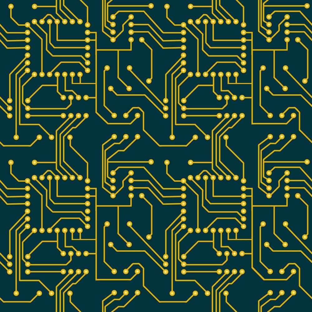
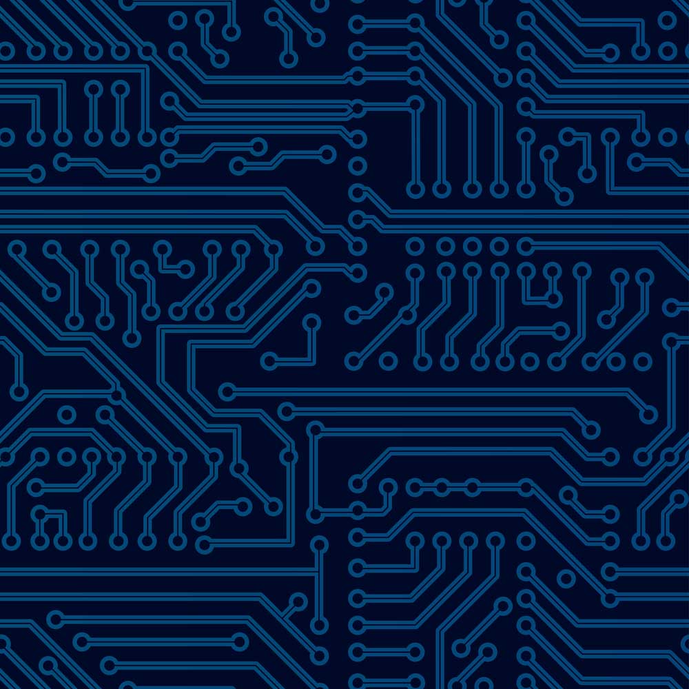
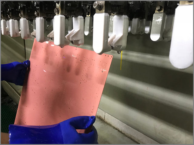 Image 3: PCB Copper Weight
The final section describes the process of calculating the copper weight. This section is about heavy and EXTREME copper's role in PCB design.
As mentioned earlier, heavy copper and EXTREME copper are considered more than ever because testing revealed that they could be soldered into a PCB without anything detrimental.
It revealed a couple of things. First, it showed that the larger thickness of heavy and EXTREME copper made most PCBs last longer than if built with standard copper.
The other thing is that placing heavy and EXTREME copper in the right areas on a PCB improves longevity. It also enhances the design by replacing the smaller standard copper weights.
It makes the creation of PCBs a lot less complicated.
6.1 How copper weight impacts PCB manufacturing
Copper weight is crucial in PCB manufacturing because of a couple of significant factors that affect how the PCB will carry a charge: Current, which is measured in amps, and impedance, which is measured in ohms.
It is easy to detect current and impedance in standard copper. It becomes a little more complicated when working with heavy and EXTREME copper.
True to their names, heavy and EXTREME copper is thicker than standard copper and has much stronger conductors.
Thus, the current and impedance of heavy and EXTREME copper have different rates that are much stronger. While this will last much longer than the charges that standard copper yields, it also means that other things must be done to maintain their proper weights on a PCB.
While standard copper can be placed on all PCB layers, heavy and EXTREME copper can only be placed on the outer layers. It creates what is called a "Powerlink."
This Powerlink can eliminate the need for multiple standard copper plates on a PCB by placing fewer heavy or EXTREME copper plates on them.
At first, creating and manufacturing PCBs using heavy and EXTREME copper may take a lot more time and effort.
But it is well worth it, as the PCB itself will look much better and be as efficient as PCBs using standard copper, if not more.
Once creating Powerlink becomes routine, you will not look back.
7、Conclusion
OurPCB is one of the leading sources of free information about PCB manufacturing and production.
If you have general issues with PCB manufacturing and production, take some time to explore other articles such as this one.
There is a good chance you will find information that will help you.
If you seek even more detailed information and feel like it would be more beneficial to acquire even more detailed information than this, do not hesitate to contact us or schedule a consultation.
We are happy to provide you with any information about any PCB components you are experiencing.
As well as information, we also provide sales and service for any materials that involve PCBs, copper included.
We contain a full catalog of materials and repair services. Please get in touch with us if necessary.
Special Offer: Get $100 off your order!
Email [email protected] to get started!