In the world of technological advancements, it can be difficult to pick a gadget that best suits you. Consequently, determining a worthwhile tester for your circuit board can be tedious. Almost always, a tester predicts the future sustainability of your board. Therefore, the ICT Test helps run tests on your brand-new Printed Circuit Board, check for defects, and correct them in advance.
Despite the market having several test methods, we’ve assembled a competent one: the In-Circuit Tester. It not only produces error-free circuit boards but also ensures they are of perfect quality. Let’s delve in deeper and learn broadly about ICT.
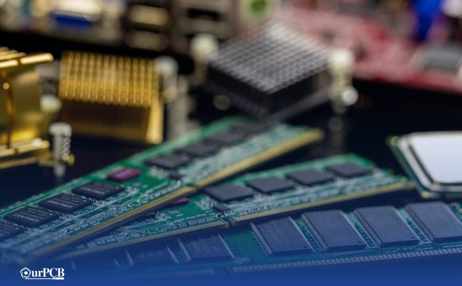
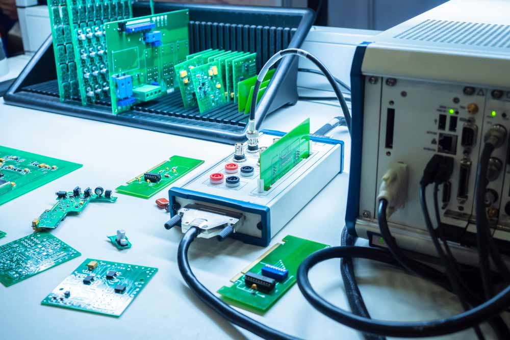
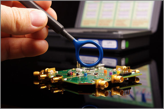
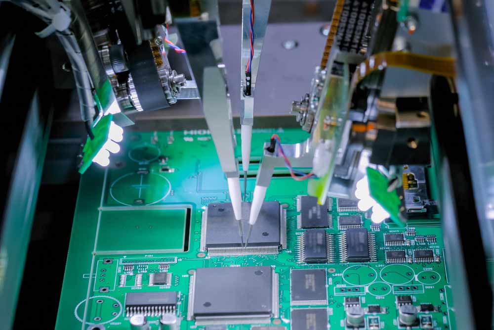
( a close-up on an ICT)
Contents
- What is ICT testing?
- Primary Types of In-circuit Testing
- Component Placement and Implementation
- Circuitry
- Component Condition
- Electrical Functionality
- The Main Types of ICT Machines you need to know.
- Standard ICT machine
- Manufacturing defect analyzer, MDA
- Cableform tester
- Flying probe tester
- Equipment Required for ICT test
- In-circuit tester
- ICT fixture
- Software
- Possible Equipment You Can Add To Your ICT Test
- What problems can we find using ICT testing?
- Power-off tests tend to detect these problems;
- Power-on tests detect;
- Example ICT Test Sequence
- The Cost of an ICT Test
- The Advantages and Disadvantages of the ICT Test
- Advantages of ICT testing
- Disadvantages of ICT testing
- Comparison of ICT Test and Flying Probe Test
- Similarities between the In-circuit Test and Flying probe test:
- The difference between ICT and FPT
- In-Circuit Test vs. Functional Test
- These situations are more suitable for using ICT tests.
- How to choose the right PCB test method
- Upfront cost and unit cost
- Coverage
- Development preparation time
- Customized
- Ability to adapt to various designs
- Expected quantity
- Budget
- PCB design/complexity
- Leading development time
- Design for Testability
- Summary
What is ICT testing?
ICT, in the circuit board technology, is an abbreviation for In-Circuit Test. It's also known as the bed-of-nails In-circuit test.
Structurally, it is an example of white box testing whereby an electrical probe tests a populated printed circuit board and checks for faultiness such as shorts, opens, etc.
Ideally, you can perform this test with a bed of nails type test fixture or featureless in-circuit test alignment.
This test method checks errors that may occur while fixing components onto the board. In doing so, you can easily replace any defective part. Moreover, it offers a fast and straightforward way of assessing the PCB board maker and providing accurate results. ICTs can also utilize suction cups to check the soldiers’ sturdiness and the malleable strength of chips.
Some known examples include but are not limited to;
- Acculogic Scorpion ICT 7000
- TRI TR5001 Inline ICT
- Automated ICT systems
How it works: first, your manufacturers will press the PCB down on a fixed bed of probes. These probes have their designs fitting a particular circuit board. After that, needles will shoot up from the bottom and be in contact with the circuit. Lastly, boards access those pins and then use them to measure the values of the PCBs.
Since it is a fully automated test, it doesn't require much human involvement other than pressing the 'start' button. Moments later, carefully measured values decide whether the test was a fail or a pass. . If you need of top-notch PCBA services with reliable PCBA testing methods, we at OurPCB are ready to assist you.
(Quality control of printed circuit boards.)
Primary Types of In-circuit Testing
In-circuit testing checks various components of the PCB, including the following.
Component Placement and Implementation
ICT testing hardware connects to specific test points on the PCB to link to components via the circuit and assess their function. In the process, the test equipment checks if the board has the right components and if they are in the right spot in the circuit.
Electronic components undergoing testing in PCBs
Circuitry
Some of the primary faults that ICT equipment tries to detect are short and open circuits. As circuit boards become tinier with slim transmission lines in multiple layers, it has become difficult to detect these circuitry errors.
Component Condition
This test can scan the board for poor-functioning or damaged components while checking if these parts are in the right place for quality control.
Electrical Functionality
In addition to checking for short and open circuits, ICT scans other electrical functions like capacitance and resistance by running specific electrical current levels through the mounted components.
The Main Types of ICT Machines you need to know.
There are several different types of ICT machines in the electronics manufacturing industry. The machine type is usually dependent on the;
- the manufacturing or testing process,
- the volume of purchased PCBs and,
- types of PCBs in the picture.
The main types of ICT machines include;
-
Standard ICT machine
In normal circumstances, this is the general test in this form of testing. However, they're standard because they offer elemental resistance, capacitance, and some device functionality.
-
Manufacturing defect analyzer, MDA
MDA offers an essential ICT of resistance, continuity, and insulation. Manufacturers use it to detect defects such as shorts and open circuit connections on the board. It uses the printed circuit board CAD data to generate the fixture design and test programs while operating. Thus, you can automatically produce about 80% of the programs.
-
Cableform tester
As the name suggests, you use its operation to test cables optimally. It works similarly to an MDA but differs in high voltage usage. The high voltage is for periodic testing for the insulation.
(cable form tester)
-
Flying probe tester
A roving or flying probe has a simple, inexpensive fixture that holds the board. A testing team then connects via a few inquiries that move around the board and make contact as needed. Often, software control monitors the movements of the probes. Therefore, any board updates will lead to a change in the software program.
(a flying probe tester)
When choosing a type of ICT machine for your products, consider the following elements common in all ICT testers. They include; controller, software, interface, fixture, analog scanner, powered analog tests, and analog-digital opens. At all times, the mentioned elements steer the operation of ICT.
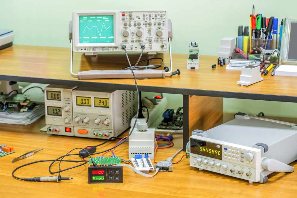
Equipment Required for ICT test
ICT equipment has several elements. The three major ones include an in-circuit tester, fixture, and software. A tester is applicable in a variety of boards, while the institution and software are board specific.
-
In-circuit tester
The system has a background of sensors and drivers that set up and perform the measurements. The driver sensor points, which are about 1000 in number, are always accessible via a large connector.
-
ICT fixture
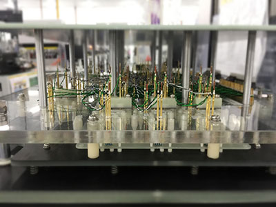
The ICT system connector is closely connected to the fixture. Manufacturers specifically design fixtures for precise boards. Functionally, the fixture acts as a connection point between the board and the tester. Initially, the institution takes connections from sensor points and conveys them to relevant board points using the bed of nails.
-
Software
Each board type has software which gives instructions on the kind of tests you need to perform. Additionally, it educates you on the processes of handling the ICT and enables you to determine if a test was successful or not.
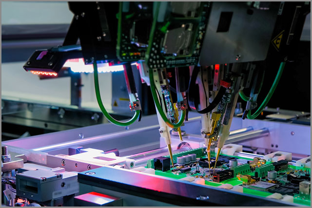
(Automation machine equipment for quality testing of printed circuit boards -ITC test at the factory)
Possible Equipment You Can Add To Your ICT Test
You can include bead-probe technology to test tiny traces that are inaccessible by the probes in the bed of nails. An external timer counter will also be handy to test components operating at high frequencies (over 50MHz), while a signal waveform analyzer will help check the envelope curve and slew rate.
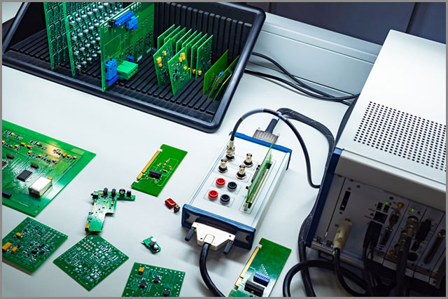
An electronics workbench with different testing equipment
A camera can also assist the ICT equipment to check the orientation or component placement correctness, while photodetectors can inform you if the LEDs in the circuit are glowing in the correct color and intensity.
If the ICT equipment cannot handle high voltages above 100V DC or AC, the source for external equipment like ICT controllers can interface with a computer to analyze the results.
What problems can we find using ICT testing?
Manufacturers perform ICT tests in two ways; when there's a supply of power or before power is applied.
Power-off tests tend to detect these problems;
- Shorts between component leads
- Open circuits where electrical continuity is cut short
- Absence of passive components
- Lack of active analog components
- Altered degrading values on the resistors
- Jumpers
- Check for missing non-electric components.
Power-on tests detect;
- Wrong analog component
- Wrong digital component
- Misoriented analog and digital component
- Capacitance and inductance values. It occurs if there’s excessive board flexure due to inadequate support placement or high probe forces.
- Transistor beta
- Stuck process bus
- Diodes and Zener diodes
- Fuses and switches
- Excess solder
 (Electromagnetic compatibility (EMC) engineers perform EMC troubleshooting and measurement)
Special Offer: Get $100 off your order!
Email [email protected] to get started!
Example ICT Test Sequence
Begin by discharging the capacitors, especially the electrolytic type, for measurement stability and safety. Next, contact the test bed, then check for open and short circuits.
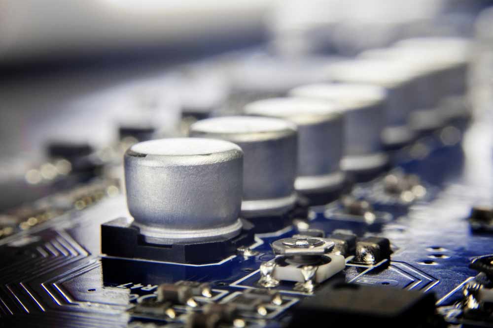
Aluminum electrolytic capacitors on a PCB
The second test should be for analog components, where you should check their value correctness and placement. After that, test the defective open pins, followed by the capacitor orientation.
Once this first phase is over, power up the PCB (unit under test), then check the analog components like op-amps and voltage regulators followed by the digital parts.
Wrap up the testing sequence by conducting JTAG boundary scans and testing the memory (EEPROM, flash memory, etc.). As you discharge the PCB after testing, discharge the capacitors, as well.
The Cost of an ICT Test
Several factors contribute to the cost of ICT. They're inclusive of;
- Volume; without a doubt, testing one type of PCB is cheaper than doing the same to various of them. For instance, 15 identical PCBs cost less compared to 15 different circuit boards.
- Board size; Logically speaking, a smaller circuit board with smaller measurements and a bed of nails leads to a lowered fixture cost.
- Board complexity: The more complex the board, the higher its cost. Complex boards also require an elaborate bed of nails, which ultimately increases the cost.
- Time; so far, manufacturers are confident about ICT being the fastest tester. Usually, it takes less than a minute to get the results. You can test more than one PCB simultaneously, depending on the design and spacing.
An average ICT is $20000 with a range of $10000 to $50000, but this is highly dependent on the factors mentioned above.
The factors above are added advantages to using ICT over other testing methods since it saves money in the long run, as it has long-term efficiency.
The Advantages and Disadvantages of the ICT Test
In a like manner to all technologies, ICT has its downsides and upsides. Even though the advantages of ICTs offset the disadvantages, knowing the advance’s expectations is crucial.
Advantages of ICT testing
ICT has some significant advantages that have been the reason manufacturers have opted for it for centuries.
They include;
- In contrast to the AOI and flying probe testers, it can test the ball grid array assemblies (BGAs).
- Straightforward interpretation; the ICT system quickly locates the faultiness and presents it to you in a matter of minutes. You may not need professionally skilled personnel to proceed with the interpretation.
- Fast/ Time-effective: It roughly takes 1 minute, compared to a flying probe tester, which may take about 25 minutes. Being short is regarding contacting all the board’s test points at once.
- Easy program generation; an ICT tester is effortlessly programmed. In that, you can take files from the PCB outline to make the essential program.
- It can test functionality as well as assembly defects as ICT systems can handle complex testing methods.
- Cost-effective: The high speed helps in quick recovery of the expense of setting up the fixture and program. It is especially true when considering boards that you assemble in large volumes.
- ICT platforms: The testing platform for ICT is available in both Windows and UNIX OS, making it universal.
- The testing can carry out several tests without applying power to the Device Under Test (DUT). It ensures a safe test and protects the board from any damage.
- Coverage: For manufacturing defects, it has high failure coverage. A more straightforward explanation for the increased range is the board’s complexity.
Disadvantages of ICT testing
- Cost; high capital expenditure in the initial purchasing.
- High densities: PCB densities can make probing difficult.
- Maintenance: The test pins require regular cleaning and replacement.
- Accessing components; other components may shield some details so that you can't achieve test access. It is to say, it can, for example, be difficult for ICT to sense low-voltage digital logic levels accurately. Their components may shield some features.
- Most, if not all, equipment manufacturers sometimes offer an expensive support contract.
- Test contact failures may occur if the test pins do not make proper contact with the appropriate test pads.
- Product preference; not apt for small-batch products where test fixture/ programming cost may be prohibitive.
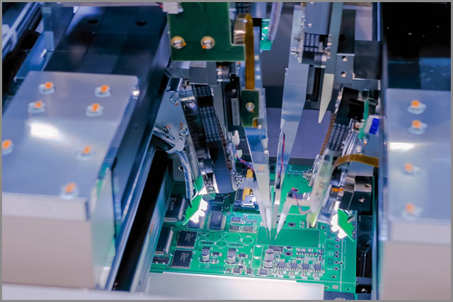
(After assembly, automated robotic equipment is using light and laser technology to test electronic printed circuit boards)
Comparison of ICT Test and Flying Probe Test
ICT testing and flying probe tests are popular test methods that often leave circuit board buyers in a dilemma. They usually prefer gauging the two’s features through their similarity, differences, advantages, and disadvantages. They are both used to test out PCBs, but they work differently.
Upon consulting, your manufacturer may help you narrow down your analysis based on the two tests by looking into;
- Costs
- Customization.
- Scope of coverage
- Ability to adapt to various designs
We will further discuss the above meanings in detail.
Similarities between the In-circuit Test and Flying probe test:
- They can all detect defects, such as; short circuit, open circuit, capacitance resistance, and component orientation.
- They both have similar samples required for the development and testing of circuit boards.
- Their power rail measurements are similar.
- They can perform passive tests involving measuring PCB values.
- In both of them, Both CAD and schematic can execute them.
The difference between ICT and FPT
Flying Probe Test and In-Circuit Test differ in the following ways:
- Test period- an ICT takes about 1 to 2 minutes for the test to get done. On the other hand, FPT takes 15 minutes.
- Per unit cost- the cost of purchasing a unit in ICT is relatively cheaper compared to an FPT. It is because the duration taken in FPT testing is longer.
- An ICT uses a bed of nails, whereas; an FPT uses many movable and fixed probes.
- FPT is suitable in the early stages of circuit board development and low quantities. Contrarily, ICT is very desirable in complex circuit boards and high-dose applications.
- ICTs test the ball grid array assemblies (BGAs) while the Flying probe tests FPGAs.
- Custom tooling- FPT requires no custom tooling, whereas an ICT does.
- Up-front costs and development lead time with ICTs are higher and longer than the ones in FPTs.
- ICT provides limited analog and digital measurements that FPT can't do due to the few probes.
- Flying probe testers can rapidly test assembly prototypes.
In-Circuit Test vs. Functional Test
ICT is effective at identifying manufacturer defects because it verifies the circuit’s schematic by testing individual components while mounted on the board. Therefore it requires a bed with more nails or more pogo pins to handle the components individually while comparing them to a software model that has the parameters of each piece. This test is not done at speed and does not check the interoperability of the circuit.
An automated testing system (flying probe)
In contrast, functional testing is done at speed to check if the circuit's functionality and interoperability meet the required specifications. The process requires a bed of nails or DUT connectors, but the nails or pogo pins are significantly less than what you need for ICT because you are testing the circuit as a whole, not each component.
These situations are more suitable for using ICT tests.
ICT testing is preferable on surface mount technology (SMT). Other than that, if you’re planning on using ICT for a long time, you will need to have these in mind.
It’s alternatively suitable if;
- You plan to insist on continuous product design for 3-4 years.
- Products purchased in large quantities. In this way, you can quickly diffuse the upfront cost during your purchase. Besides, ICT can test more than one circuit board at the same time. A low order would mean a waste of your money if you run out of testing products.
- Long product life. ICT tests are known for quality testing. In the long run, ICT will heighten your products' longevity.
How to choose the right PCB test method
-
Upfront cost and unit cost
Upfront cost is the payment made in advance to the manufacturers before the testing and inspection start.
Unit cost: It is an expenditure incurred to produce, store, and sell one department unit of a particular product or service.
The cost also includes the maintenance you'll need to make on the PCB once in a while. For instance, even if your product design changes, you may only need a program change. In ICTs, however, you will need a new fixture and components.
The programming cost frequently depends on the complexity of the board assembly process but is often the same for test solutions: about £2000. Other charges vary with the test method itself and the PCB in question.
For example, FTPs' fixture costs are zero because they are fixtureless, while ICT fixtures can cost up to £4000.
-
Coverage
Coverage means how much of the circuit board you can test. Both ICT and FTP carry out Manufacturing Defects Analysis (MDA). It allows for defects that are likely to occur, such as open circuits, shorts, diode, transistor orientation, and voltage measurement.
As an illustration, most FPTs offer some form of limited optical inspection that adds to the coverage of components that can't be accessed electrically.
-
Development preparation time
It refers to the length of time a PCB testing method takes during the circuit board or project’s basic check-up.
-
Customized
Manufacturers specifically design customized test products according to the buyers’ desires or specifications. On that note, you’ll find different test methods possessing varied shapes, sizes, features, etc., that best fits your board.
-
Ability to adapt to various designs
A PCB test method that adapts to various circuit board designs enables a manufacturer to test diverse boards with no limitations. PCB designs contribute to the functionality and regulatory process of the panels. Thus, a high adaptivity will highlight the board’s quality.
-
Expected quantity
You can use some test methods with large-scale type products. With others, it is preferable to have a small number of products. For instance, ICTs test large quantities of PCBs, often at the same time. Yet, FPT’s test a small amount as it has limited features.
-
Budget
A test method’s budget estimates the expenses you need to cater for over a specific time. Let's say you want to use an ICT test; you will need to evaluate a 3 to 4-year budget for the machine or procedure. That will include all the equipment you are to use.
-
PCB design/complexity
A quality test program relies on the quality of your Computer-Aided Design data and schematics. CAD data generates the basic test program and ensures you source the information from the original board design. Quality dense and unpopulated PCBAs are essential for tuning in the programs and making any fixtures. Consequently, this ensures the assemblies physically fit as intended.
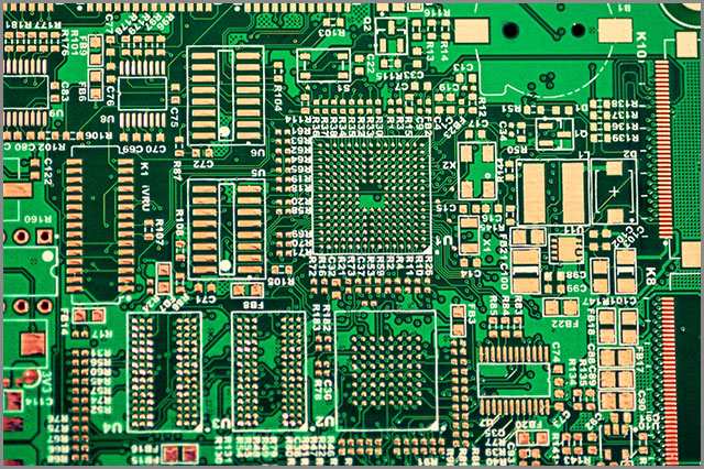
(an intricate PCB design)
-
Leading development time
Running times for test methods differ. As such, you'll have a flying probe test having an average lead time of 5-15 minutes. Some other larger boards can take 30+ minutes with the same method, but that rarely happens.
Design for Testability
Since ICT is an automated testing process, you have to design the PCB optimally for connectivity to the testing equipment to ensure complete coverage. So PCB designers should consider including precise location and tooling holes for firm and correct PCB placement in the test equipment.
The test pads should be easy to connect to probes, as well, to provide electrical access to each net. Try to make them at least 30 mils in diameter, but if the board has very little real estate to spare, aim for 24 mils and use guided probe fixturing. Also, ensure these pads are at least 0.0125 inches from the edge of the PCB.
For ground testing, allocate about 10% of the nodes for this function and distribute them evenly across the PCB. In addition to test pads, prioritize connection points like via-holes and through-hole component leads and include tooling holes on the breakaway strips of panelized PCBs.
Summary
To conclude, I firmly believe your next move on getting your PCB products tested by an ICT will be simple. Remember, a tested circuit board is far more efficient and more comfortable to sustain. Get your board tested and save yourself a long period of peace.
Whether you are a PCB buyer, manufacturer, or distributor, we have to ensure that you feel at home and gain the best experience with our articles. In case you have any questions regarding ICTs and clarification of matters, kindly reach out to us.
We work around the clock. Meaning, we will be able to get you back. We are always alert to help you sort out your circuit board needs.
Special Offer: Get $100 off your order!
Email [email protected] to get started!