The OurPCB team created two tables mapping PCB failures into DIY Hobby PCB Failures and Commercial PCB Assembly Manufacturing Failures:
Contents
DIY PCB Failures
DIY failures often stem from improper handling and design errors, while commercial manufacturing failures are more likely related to fabrication defects and large-scale assembly challenges.
| DIY Hobby PCB Failures | Failure causes |
|---|---|
| Physical Damages | Water exposure, dust buildup, accidental drops, oxidation, vibration, heat damage |
| Design Flaws | Incorrect component placement, poor trace design, improper material selection |
| Soldering Defects | Cold solder joints, insufficient solder, bridging, flux contamination |
| Thermal Issues | Overheating due to improper heat dissipation or lack of thermal vias |
| Open/Short Circuits | Misaligned traces or solder bridges causing connectivity issues |
| Copper Issues | Copper traces too thin or too close to board edges |
| Ionic Contamination | Residues from poor cleaning causing corrosion or electrochemical migration |
| Pad Lifting | Pads detaching due to excessive heat during soldering |
| Burned Components | Overheating components due to incorrect power supply or soldering errors |
| Environmental Factors | Heat, dust, moisture exposure during DIY handling |
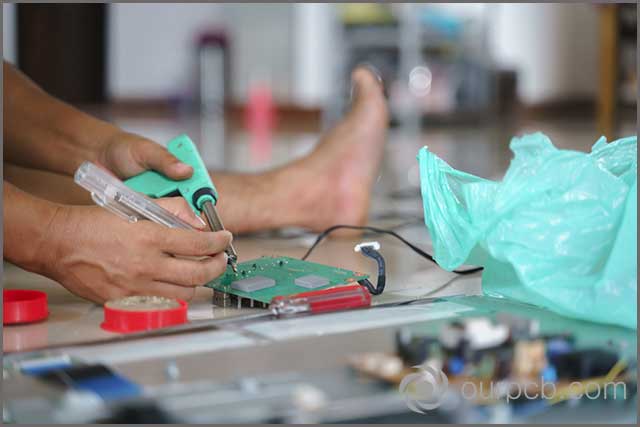
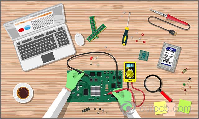
(A technician fixing a broken PCB)
Commercial PCB Assembly Manufacturing Failures
| Failures of Manufactured PCBs | Failure causes |
|---|---|
| Manufacturing Errors | Over-etching, drilling errors, misaligned layers, insufficient clearances |
| Plating Voids (Fabrication) | Holes or gaps in circuit board plating due to deposition issues |
| Acid Traps (Fabrication) | Acid buildup in acute angles during etching |
| Thermal Issues (Design & Assembly) | Starved thermals, overheating due to poor thermal management |
| Electromagnetic Issues (Design) | Poor trace layout causing EMC/EMI problems |
| Soldering Defects (Assembly) | Cold soldering, black pad defects, outgassing |
| Conductive Anodic Filament Formation (CAF) | Electrical failure due to conductive material growth |
| Interconnect Defects (Fabrication) | Separation between copper filler and circuits |
| Measling and Delamination (Fabrication) | White spots or bubbles due to poor lamination |
| Aging (Components) | Component fatigue or breakdown over time |
| Chemical Leakage (Components) | Corrosion or shorts caused by leaked chemicals |
| Mechanical Failures (Assembly) | Warpage, deformation, brittle fractures |
| Electrical Stress Failures | Electrostatic discharge (ESD), dielectric breakdown, overvoltage |
| Packaging Failures (Components) | Cracks or overstressed wire bonds |
| Slivers (Fabrication) | Thin pieces of copper or solder mask causing shorts |
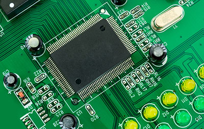
(Electronic circuit board, Setup IC)
Special Offer: Get $100 off your order!
Email [email protected] to get started!
Comprehensive Failure Analysis Techniques
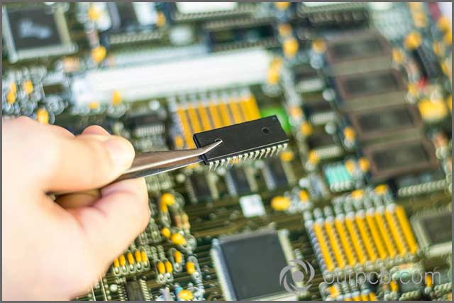
(PCB Failure Analysis)
To address PCB failures effectively, a systematic failure analysis approach is critical:
| Technique | Purpose | Tools Used |
|---|---|---|
| Electrical Testing | Identifies open/short circuits | Probe stations, functional testers |
| Signal Integrity Analysis | Diagnoses waveform issues | Oscilloscopes |
| Emission Microscopy | Detects hotspots from resistance | Infrared cameras |
| Thermal Profiling | Identifies overheating components | Thermal scanners |
| Chemical Analysis | Reveals hidden defects | Chemical etchants |
| Cross-sectioning | Inspects internal layers | Microscopes |
How to Prevent Failures?
| Failure Mode | Prevention Strategy |
|---|---|
| Cracks/Bends | Prebaking, humidity control |
| Polarity Issues | Diode protection, proper labeling |
| Solder Joint Fractures | Automated soldering, visual inspection |
| Corrosion | Thorough cleaning after assembly |
| Short Circuits | Electrical testing, reduced stencil thickness |
| Copper Weight Issues | Follow design specifications |
| Component Misalignment | Accurate pick-and-place machines |
| Low Warranty Components | Source high-quality parts |
| Dewetting | Cleaning and surface preparation |
By following these best practices and leveraging advanced failure analysis techniques, manufacturers can significantly improve PCB reliability while minimizing rework costs and customer dissatisfaction.
References to Internal Links
- For more information on Printed circuit board assembly, visit our detailed guide.
- Learn about flex electronics and their applications.
- Explore our services on PCB manufacturing.
- Check out our PCB trace design guidelines.
- Discover our circuit board solutions.
- Find out about our PCB assembly services and request a prototype.
OurPCB is willing to provide services on PCB and PCBA. You may ask for an online quote or email us to get in touch with our engineers.
Special Offer: Get $100 off your order!
Email [email protected] to get started!