Contents
What is the difference between PCBA and PCB?
The main difference between PCB (Printed Circuit Board) and PCBA (Printed Circuit Board Assembly) is that a PCB is a bare board with electrical pathways, while a PCBA is a PCB with components installed, soldered, and tested for functionality. PCBs are cheaper and faster to produce as they only require fabrication, whereas PCBAs involve assembly, soldering, and testing, leading to higher costs and longer production times. PCBs serve as the foundation for all electronics, while PCBAs are complete, functional systems ready for integration into devices.
| Factor | PCB | PCBA |
| Definition | Printed circuit boards are rigid or flexible boards consisting of copper layers sandwiched in insulative materials. | PCBAs are assembled PCBs (with components mounted and soldered). |
| Parts | Does not have any assembled components. The bare board only has the circuit traces. | Has all the components assembled on the board. |
| Functionality | The board only provides a circuit for mounting and interconnecting the components. | PCBAs are complete devices that are ready for integration into the application area. |
| Manufacturing | Manufacturing encompasses design, fabrication, and PCB testing. | Doesn’t involve any manufacturing. Just component mounting, soldering, and testing. |
| Complexity | Single-layer boards are simple but multilayer PCBs with tightly-packed traces and many interconnections are complex. | The component assembly and type (through-hole vs. surface-mount). |
| Cost vs. Time | Can be affected by different factors but PCBs are generally cheaper and faster to produce. | Making a PCBA involves PCB fabrication, so the overall cost and lead time is higher. |
| Flexibility | PCBs can be flexible, rigid, or rigid-flex. | Same as PCBs (flexible, rigid, or rigid-flex). |
| Assembly Processes | Does not require assembly. | The primary assembly types are wave (for through-hole) and reflow (for surface mount), but you can use manual soldering, as well. |
| Durability | This factor is mostly determined by the construction material. | The PCB’s construction material plays a role in a PCBA’s durability but the quality of the assembled components matters, as well. |
| Applications | PCBs are the foundation for all modern electronic devices. | PCBAs are assembled PCBs, so their applications are the same, but these are complete, fully-functional devices. |
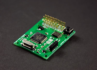
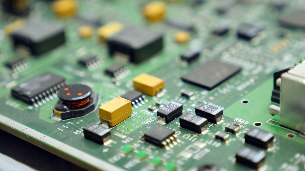
A PCBA with capacitors, resistors, and integrated circuits mounted on the PCB
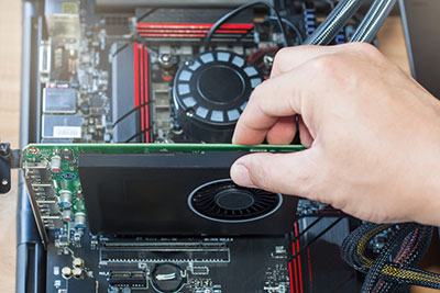
What is PCBA (Printed Circuit Board Assembly)?
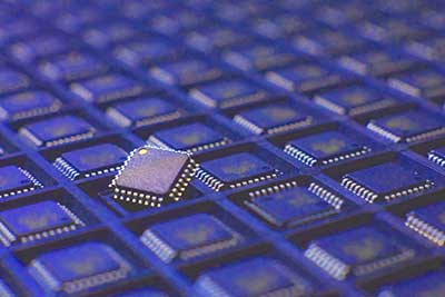
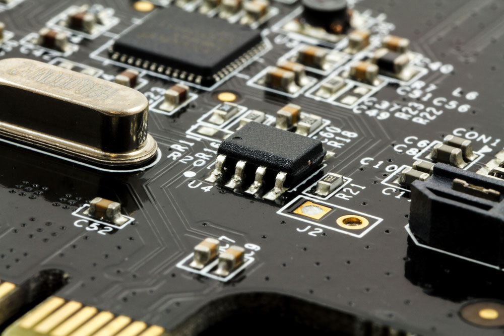
PCBA is an acronym that stands for Printed Circuit Board Assembly. PCBA is what you get when all the components are attached and soldered onto a printed circuit board (PCB). This process involves placing and soldering parts like resistors, capacitors, and integrated circuits onto the PCB. PCB assembly is a crucial step in electronics manufacturing, transforming a bare PCB into a complete, working circuit ready for use in applications ranging from consumer electronics to industrial machinery. Understanding the different aspects of PCB fabrication and assembly is essential for ensuring quality and reliability in your projects.
Special Offer: Get $100 off your order!
Email [email protected] to get started!
PCB Assembly Methods
Thru-Hole Technology
This involves mounting components by drilling holes into the PCB and inserting leads, such as coils and capacitors. This method creates a strong bond between the board and its components.
Mixed Technology
Mixed Technology combines Thru-Hole and Surface Mount components in modern PCBAs to accommodate complex circuits. This method includes a mix of components like capacitors, integrated circuits, coils, and resistors.
Surface Mount Technology
Surface Mount Technology attaches electronic components directly to the surface of the PCB. This fully automatic process allows for higher assembly densities by fitting complex circuits onto small boards.
What are the benefits of PCBA?
Following the latest advancements in electronic manufacturing, PCBA offers several advantages that enhance both efficiency and reliability. Here’s how PCBA benefits your projects:
- Saves Time: PCBA (Printed Circuit Board Assembly) is much faster to build compared to connecting components with wires.
- Compact Design: PCBAs allow for a smaller and more efficient design by packing multiple components into a compact space.
- Maximizes Durability: With no hanging wires to get damaged, PCBAs are more durable and reliable.
- Simplifies Repairs: Replacing a faulty component is easier on a PCBA than dealing with numerous wire connections.
- Affordable: PCBAs are cost-effective to produce, which helps keep project costs down.
FAQs about PCBA
What are the applications of PCBA?
Printed Circuit Board Assemblies (PCBA) are essential in various sectors:
- Medical Devices: Used in diagnostic and therapeutic devices for reliable and precise operations.
- Automotive Electronics: Essential for control systems in vehicles to enhance functionality and safety.
- Electrical Equipment: Improves the efficiency and reliability of various electrical devices.
- Military and Aerospace: Key component in communication and navigation systems, ensuring robust performance.
- Consumer Electronics: Foundational in enhancing the functionality and performance of devices like smartphones and computers.
- Safety and Security Systems: Used in advanced control and monitoring systems to ensure security and compliance.
- Maritime Technology: Critical in navigation and control systems aboard ships, enhancing safety and operational capabilities.
How to Choose Between PCB and PCBA
Choose a PCB if you need a basic, unassembled board for custom assembly or prototyping. Opt for PCBA if you want a fully assembled board with all components included, saving you time and effort. PCBA is ideal for ready-to-use solutions and mass production, while PCB suits those who prefer to assemble their own components.
Get in Touch
Back to Top: What is PCBA?
Special Offer: Get $100 off your order!
Email [email protected] to get started!