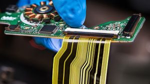
Prototype Cable Assemblies
Prototype cable assemblies are the very important place in between PCB design ideas and interconnects. OurPCB brings prototype assemblies with PCB solutions to your tables.
 5 Star Rating on

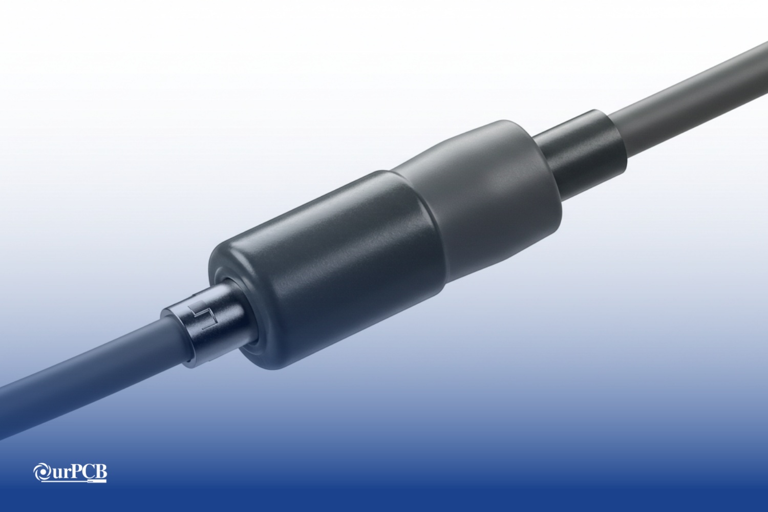
Overmolded cable assemblies provide the best environmental protection. It does this through precision injection molding processes that cover cable terminations in protective thermoplastic materials. OurPCB delivers custom solutions achieving IP67/IP68 environmental ratings. Our products come with 360-degree strain relief for medical devices, aerospace systems, and industrial automation equipment.
Traditional assemblies can give up on you without proper environmental sealing and sufficient strain relief. This can cause moisture ingress, corrosion, and electrical failures. Our overmolding technology creates unified, sealed construction that protects internal connections from environmental contaminants, mechanical stress, and electromagnetic interference.


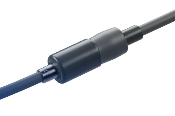

Overmolded cable assemblies is a cable assembly process that uses injection molding technology to completely encapsulate cable and connector junctions with thermoplastic materials, creating integrated protective units. The molding process involves placing pre-assembled connections into precision molds and injecting molten materials under high pressure to form protective shells. This transforms standard cable assemblies into environmentally sealed, mechanically reinforced interconnect solutions that eliminate external element penetration.
The two core construction methods are two-shot molding and insert molding. We break both down below for your mold tooling.
The inner mold encapsulates termination points, preventing wire floating. The outer overmold provides environmental protection. It enables multiple molding material combinations for cost optimization.
The insert molding technique is a manufacturing method. It is a single-shot process for specific geometries. It allows precise cable positioning within the mold cavity. It ensures consistent wall thickness and strain relief geometry.
The complexity of tooling allows for sophisticated molded assemblies with enhanced functionality compared to off-the-shelf solutions.


The benefits of molded cable assemblies are their superior performance advantages through integrated construction that provide environmental protection, mechanical durability, and electrical reliability. These benefits ensure cable assemblies withstand harsh operating conditions while maintaining signal integrity and extending operational lifespan.
We’ve outlined each benefit here in more detail for you to inform yourself:

test
OurPCB combines advanced manufacturing capabilities with comprehensive engineering support to deliver high-quality overmolded cable assemblies across all industries. Our vertically integrated approach ensures consistent quality control from initial design through finished product delivery while maintaining competitive lead times.

![]()
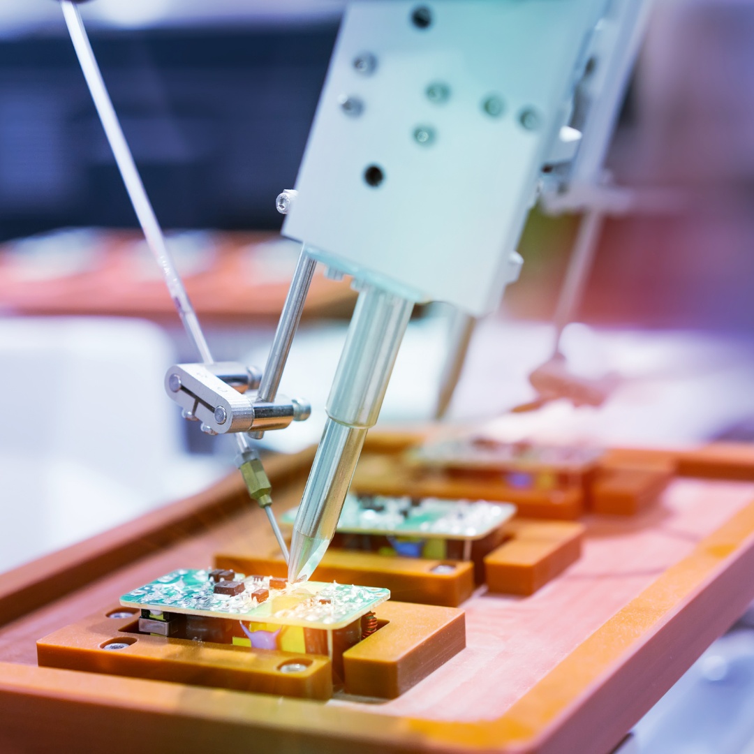
Our dual 10,000 m² PCB assembly houses in Shenzhen and Shijiazhuang are equipped with high-speed SMT assembly lines capable of placing fine-pitch parts with ±25 µm tolerance.
Each line includes temperature- and humidity-controlled environments, active anti-static systems, and vacuum transport for handling thin or flex printed circuits.
![]()
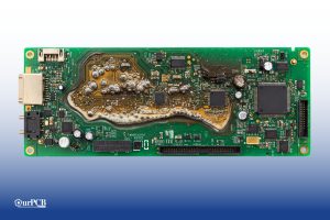
We are fully certified to ISO 9001, IATF 16949, and IPC-A-610 Class 2 & 3, supporting applications where fine-pitch PCB assembly must meet elevated acceptance criteria for solder joint geometry, lead coplanarity, and component body clearance.
Our QA workflows are built to handle fine-pitch PCBs requiring zero solder bridging and uniform joint fillets across dense arrays.
All assemblies involving ball pitch under 0.5 mm, QFN, or PoP packages undergo X-ray inspection, SPI, and AOI with 15 µm resolution optics.
We detect voids, open leads, insufficient solder, lifted terminations, and hidden shorts. This inspection process is a requirement for successful assembly when working with components that provide no visible solder access.
Every fine-pitch electronic assembly receives a DFM and DFA review focused on stencil coverage, aperture tuning, pcb design limitations, and routing near fine-pitch ICs.
We assist in verifying pad design, thermal pad exposure, and via escape planning, important for high I/O packages like BGA and chip scale layouts where misalignment or solder blockage can compromise yield.
We offer full assembly component sourcing through partners like Digi-Key, Mouser, and WPG, including traceable lots for hard-to-find or moisture-sensitive electronic components.
Components are stored under MSL-compliant conditions, with drying cabinets and vacuum packaging for all incoming fine-pitch parts.
Moldflow analysis utilizes computational fluid dynamics to simulate molding material behavior during injection molding, predicting flow patterns, pressure distribution, and potential defects before physical tool creation. Our in-house engineering team analyzes gate locations, runner systems, cooling channel placement, and material distribution to optimize molded part quality.
This predictive capability eliminates costly design iterations and ensures first-time manufacturing success.
Analysis parameters include flow simulation elements and design optimization. They are specific, measurable variables used during moldflow simulation to predict material behavior and optimize injection molding performance. These critical factors include material flow rates, pressure distribution patterns, cooling characteristics, and potential defect locations that determine final part quality.
Flow Simulation Elements:
Design Optimization:
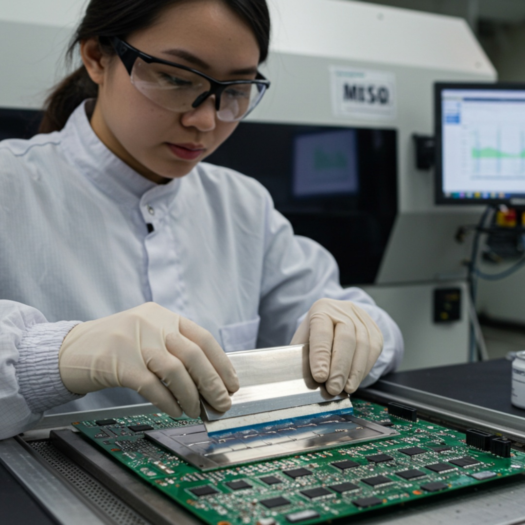
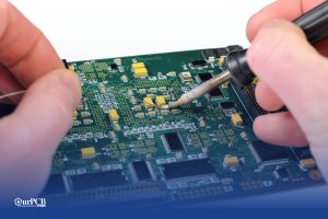
OurPCB integrates PCB testing services directly into SMT, THT, and mixed-technology production lines.
AOI, ICT, and functional test platforms are embedded at key points across our two 10,000 m² facilities in Shenzhen and Shijiazhuang.
Boards pass through automated inspection and electrical test stages without manual handling, reducing contamination risk and improving test repeatability across Class II and III assemblies.
We build all ICT and functional test fixtures internally using CAD-based modeling, high-precision CNC drilling, and pogo-pin calibration systems.
Fixtures are validated for flatness, probe pressure uniformity, and node-to-net correlation before use.
This internal control allows us to shorten test development cycles for new PCB assembly testing services and maintain consistency across repeat orders or multi-site deployments.
![]()
Our test infrastructure includes high-speed AOI (25 µm resolution), 5 µm X-ray inspection, 4-wire flying probe testers, and digital high-voltage dielectric testers.
Resistance measurements down to 10 mΩ, voltage capture from 100 mV to 1500 VDC, and insulation resistance over 1000 MΩ ensure detailed diagnostics for every PCB testing service.
Measurement integrity is maintained through ISO-calibrated instruments and logged reference values.
![]()
We provide serialized test data with barcode traceability, linking each board to its BOM revision, test station ID, operator, and timestamp.
Reports include fail point coordinates, signal path diagnostics, image references (for AOI/AXI), and environmental test logs.
Our infrastructure supports full compliance with ISO 9001, IATF 16949, and medical-sector audit requirements, making our PCB functional testing services suitable for regulated deployments.
![]()
Our testing flows conform to IPC-A-610H Class III for high-reliability electronics, including burn-in testing, dielectric breakdown validation, and full visual and optical inspection of PCBs before final sign-off.
We support test plans that include ESS, startup sequence monitoring, and functional loop stress testing to simulate real-world deployment.
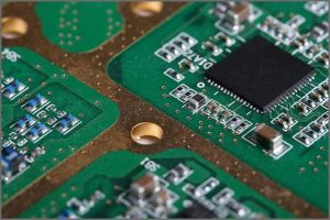
All solder joints, including BGA and QFN, are inspected using 3D AOI and void-mapped X-ray analysis.
![]()
Comprehensive quotes for PCB testing services and fixture-based setups are delivered within 48 working hours.
For new PCBA designs, we provide a DFT assessment, pin map verification, and component access review before test planning begins.
This early-stage input improves test coverage, minimizes false failures, and enables rapid onboarding for customers requiring PCB assembly testing services with complex or high-mix builds.
Analysis parameters include flow simulation elements and design optimization. They are specific, measurable variables used during moldflow simulation to predict material behavior and optimize injection molding performance. These critical factors include material flow rates, pressure distribution patterns, cooling characteristics, and potential defect locations that determine final part quality.
Flow Simulation Elements:
Design Optimization:
Hybrid overmolded assemblies combine multiple protection technologies within single assemblies, utilizing overbraided shielding with cable overmold environmental protection for applications requiring both electromagnetic shielding and environmental sealing. Low pressure molding techniques encapsulate sensitive electronics while maintaining dimensional accuracy on delicate components and PCBs.
Specialized hybrid approaches combine multiple protection technologies within single overmolded assemblies, such as overbraided overmolded designs and accordion boot integration. They can achieve enhanced performance characteristics beyond standard overmolding. These advanced techniques integrate different materials, construction methods, and protective elements.
Overbraided Overmolded Design:
Accordion Boot Integration:
Multi-Material Construction:
Custom molded cable assemblies utilize this hybrid approach to improve the performance of complex assemblies requiring specialized materials that can be used for unique assembly needs.
Thermoplastic polyurethane serves as primary overmolding material providing flexibility, abrasion resistance, and chemical compatibility. Medical-grade formulations meet USP Class VI biocompatibility standards while flame-retardant versions achieve UL94 V-0 ratings. Material selection considers operating temperature, chemical exposure, flexibility requirements, and regulatory compliance with high-reliability specifications.
| Material | Temperature Range | Key Properties | Applications |
|---|---|---|---|
| TPU | -40 °C to +125 °C | Flexible, abrasion-resistant | General purpose |
| PVC | -20 °C to +85 °C | Cost-effective, flame retardant | Industrial |
| Santoprene | -50 °C to +135 °C | Chemical resistant | Automotive |
| Polycarbonate | -40 °C to +130 °C | Rigid, optical clarity | Fiber optic |
| EPDM | -55 °C to +150 °C | Weather resistant | Outdoor |
| Silicone | -65 °C to +200 °C | Extreme temperature | Medical/aerospace |
The number of potential materials used in the overmolding process provides extensive customization options, with consideration when designing for specific application requirements and fabrication constraints.
OurPCB provides comprehensive PCB assembly solutions integrating seamlessly with molded cables, enabling complete electromechanical manufacturing under unified quality management. Assembly capabilities support control boards, interface modules, and embedded systems connecting directly to cable harness assembly applications, preventing assembly errors through integrated design and manufacturing processes.

Surface Mount Technology utilizing high-precision equipment for ±0.025mm placement accuracy with advanced vision systems ensuring proper component orientation for reliable solder joints.

Flexible options accommodate customer-supplied components or complete turnkey solutions including procurement, kitting, and assembly with supply chain management ensuring component traceability.

Complex layouts with high-density placement, fine-pitch BGAs, and specialized components supported through design for manufacturing (DFM) analysis optimizing yield and reliability while eliminating potential design conflicts.

Rapid prototyping within 3-5 business days through dedicated production lines maintaining consistent quality standards regardless of delivery timeline.

Highest reliability standards for aerospace, medical, and military applications with enhanced inspection including automated optical inspection (AOI) and comprehensive documentation packages.

Advanced capabilities handling BGAs, PoPs, CGAs, QFNs, DFNs, and CSPs with X-ray inspection verifying hidden solder joints and specialized ESD protection protocols, replacing traditional backshells with integrated protection.
Engineering capabilities encompass complete design-to-manufacturing services utilizing finite element analysis (FEA) for strain relief optimization and mechanical performance prediction. Environmental testing includes IP rating verification, salt spray testing, thermal cycling, vibration testing, and chemical compatibility assessment. Quality management maintains statistical process control with real-time monitoring of injection pressure, temperature profiles, and cycle times.
Our overmold tooling capabilities include both hardened steel production molds and aluminum prototype molds for design validation. 3D printed prototypes enable rapid validation before committing to production tooling investment. Documentation systems provide complete traceability from raw material certification through finished product inspection, supporting medical device, aerospace, and automotive quality requirements while maintaining proper tolerances throughout the manufacturing process.
OurPCB’s advanced cable expertise delivers environmental protection, mechanical durability, and electrical performance your applications demand. ISO 9001:2015 certified processes, comprehensive engineering support, and flexible volume requirements make us your ideal interconnect solution partner for robust cable applications.
Contact our engineering team for technical consultation, material recommendations, and detailed project proposals bringing your designs to life with proven overmolding expertise and vertically integrated manufacturing capabilities.
Class III testing protocols are applied to automotive electronics, implantable and diagnostic medical devices, aerospace controls, and industrial safety systems with narrow fault tolerances and redundant circuit design.
All PCB testing services in this class follow IPC-A-610H Class III inspection standards and leverage elevated inspection thresholds, including 100% AOI coverage, post-reflow X-ray validation, and ICT with 95% minimum fault coverage.
Functional tests include thermal cycling simulations, startup-sequence monitoring, and analog signal stability under full operating load. Solder joint evaluation includes BGA voiding analysis (below 25% max area) and coplanarity verification to ±50 μm on all perimeter components.
Assemblies are electrically validated using high-accuracy power supplies, 4-wire resistance probes, and embedded sensor simulation modules that replicate actual use conditions. Environmental stress screening (ESS), burn-in testing, and optional conformal coating evaluation are included in high-reliability testing packages to qualify boards for long-term deployment in regulated sectors.
Every PCB testing service performed by OurPCB is logged with time-stamped records, fixture IDs, and unique board serial numbers for traceability across production lots. We integrate barcode scanning and digital record systems to track individual assemblies through each testing process, from in-circuit verification to final functional testing.
Electrical and inspection data are output in structured formats, including CSV, XML, and proprietary report templates compatible with MES and ERP platforms. Logged values include measured voltages, pass/fail status, detected fault types, and operator annotations. AOI and X-ray inspection systems capture and archive image files linked to serial numbers, enabling post-process review and historical analysis.
Each test result is indexed to the board’s BOM revision, date code, and routing lot, allowing for full backward traceability during quality audits or field failure investigations. Our traceability infrastructure meets the documentation and retention requirements for ISO 9001, IATF 16949, and IPC Class III PCB assembly testing services, supporting consistent product quality and regulatory readiness.
Mon-Fri: 24 hours,
Sat: 9am-6pm, GMT+8
Reach us at
[email protected]
24 hours online
+86-199-30589219
Mon-Fri: 24 hours,
Sat: 9am-6pm, GMT+8
Our moldflow analysis utilizes advanced computational fluid dynamics software simulating material behavior, flow patterns, and cooling rates before mold fabrication. Analysis includes gate optimization, pressure distribution mapping, and defect prediction ensuring optimal part quality and eliminating costly design iterations through comprehensive consideration when designing complex geometries.
We manufacture hybrid assemblies combining overbraided EMI shielding with environmental overmolding, creating assemblies with both electromagnetic protection and IP67/IP68 environmental sealing. Specialized techniques include accordion boot integration and multi-material construction for demanding applications requiring enhanced durability.
Our material library includes Viton for caustic chemical resistance, EPDM for weather resistance, space-grade compounds for radiation protection, and medical-grade TPU meeting USP Class VI biocompatibility. Material selection considers temperature range, chemical exposure, sterilization requirements, and regulatory compliance needs ensuring cables withstand extreme operating conditions.
Request a quote and get a custom testing plan tailored to your design, BOM, and inspection needs. We provide PCB testing services with full traceability, calibrated measurement systems, and certified workflows for Class II and Class III assemblies.
Prototype cable assemblies are the very important place in between PCB design ideas and interconnects. OurPCB brings prototype assemblies with PCB solutions to your tables.
PCB thermal management prevents component overheating through strategic heat transfer techniques. Without proper thermal control, electronics are at risk of electronic failures through weakened solder
ContentsKey TakeawaysWhat is a Multilayer-Printed Circuit Board?How do Multilayer PCB Boards Work?Multilayer PCB ApplicationsMultilayer PCB Manufacturing Process: StepsMultilayer PCB Manufacturing MachinesBenefits of Multilayer Circuit BoardsWhat
As electronics continue to miniaturize while processing power increases, the resulting thermal challenges make high-Tg PCBs increasingly essential for modern electronic design. ContentsKey TakeawaysWhat is

Running a computer system requires computer memory. In the entire computer system, it’s one of the vital components. Therefore, it’s important that you have basic
Electronic enthusiasts developing a circuit project may want to think about whether or not they should integrate an FFC vs. FPC. Both cables possess varying
We use cookies to improve your browsing experience, which may include personal information. By clicking "Agree," you accept our Privacy Policy and cookie use. You can change your cookie settings in your browser anytime.
Agree Chat With Us
 Free Quote