Contents
- Key Takeaways
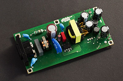
- What is a Multilayer-Printed Circuit Board?
- How do Multilayer PCB Boards Work?
- Multilayer PCB Applications
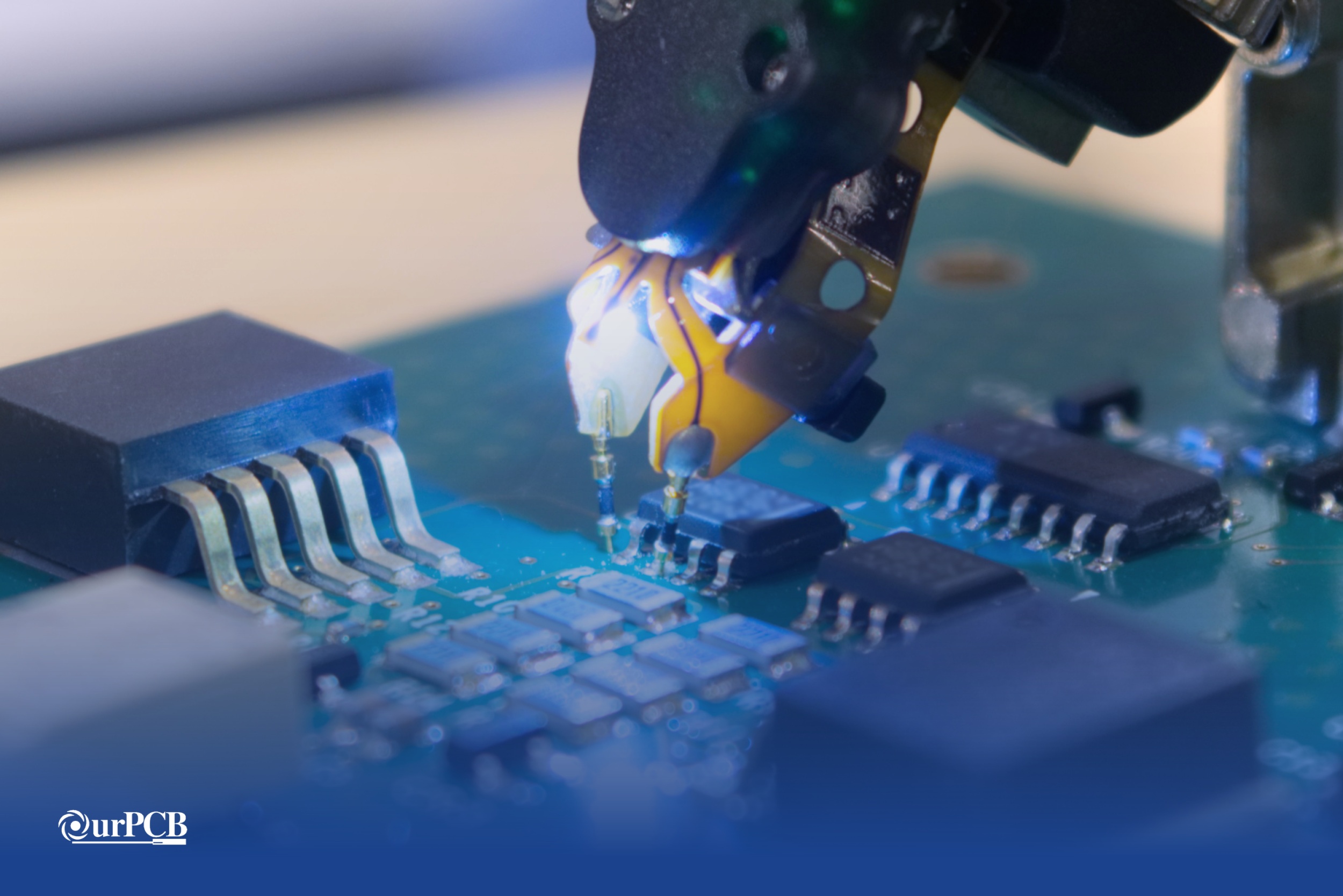
- Multilayer PCB Manufacturing Process: Steps
- Multilayer PCB Manufacturing Machines
- Benefits of Multilayer Circuit Boards
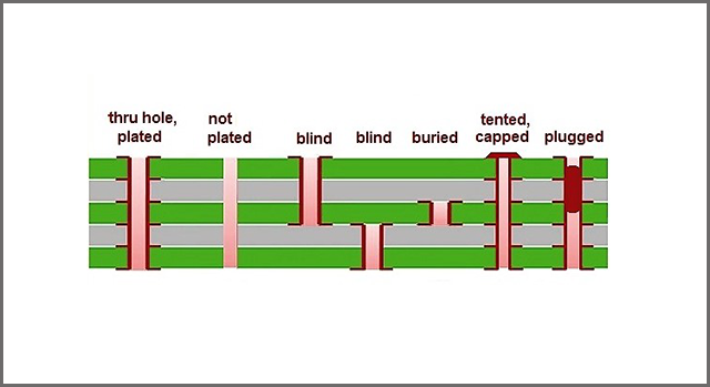
- What is a PCB Via?
- Blind Hole Via
- Through Hole Via
- Buried Via
- OurPCB: High-Quality Multilayer Boards
- FAQs on What is a Multilayer PCB?
- What is the difference between single and multilayer PCB?
- How to tell if a PCB is multilayer?
- What are the disadvantages of multilayer?
Key Takeaways
- A multilayer PCB contains three or more conductive layers.
- The manufacturing process involves precise steps for quality control.
- Multilayer PCBs are widely used in consumer electronics and medical devices.
- They offer advantages such as space efficiency and improved performance.
- Different types of vias connect the layers within a multilayer PCB.
What is a Multilayer-Printed Circuit Board?
A multilayer printed circuit board (PCB) is a type of PCB that includes multiple conductive layers. Each layer is separated by insulating material. This design allows for more complex circuitry than single or double-sided PCBs. Typically, multilayer PCBs have at least three layers, but they can have many more. The layers are bonded together to create a single, compact unit. This construction supports high-density interconnections and minimizes space requirements.
How do Multilayer PCB Boards Work?
Multilayer PCBs work by stacking several layers of conductive materials and insulating materials. Each layer has specific functions, such as routing signals or providing power. The outer layers often contain components, while inner layers handle routing and connections. Vias are used to connect different layers, allowing signals to pass through the board. This layered structure enables efficient signal transmission and reduces electromagnetic interference.
Multilayer PCB Applications
Multilayer PCBs are used in various applications across industries, such as in consumer electronics, medical devices, and more. Common uses include:
- Consumer Electronics: Smartphones, tablets, and laptops rely on multilayer designs
- Medical Devices: Equipment like monitors and imaging devices require compact, reliable circuits
- Automotive: Modern vehicles use multilayer boards for advanced features and safety systems
- Telecommunications: High-speed data transmission relies on efficient circuit designs
If you are looking for specialized services for these applications, consider the following options:
- Electronic Prototype Circuit Board & Assembly
- High-frequency PCBs for Telecommunications
- Medical PCB Assembly Manufacturer
- Automotive PCB Assembly Services
Special Offer: Get $100 off your order!
Email [email protected] to get started!
Multilayer PCB Manufacturing Process: Steps
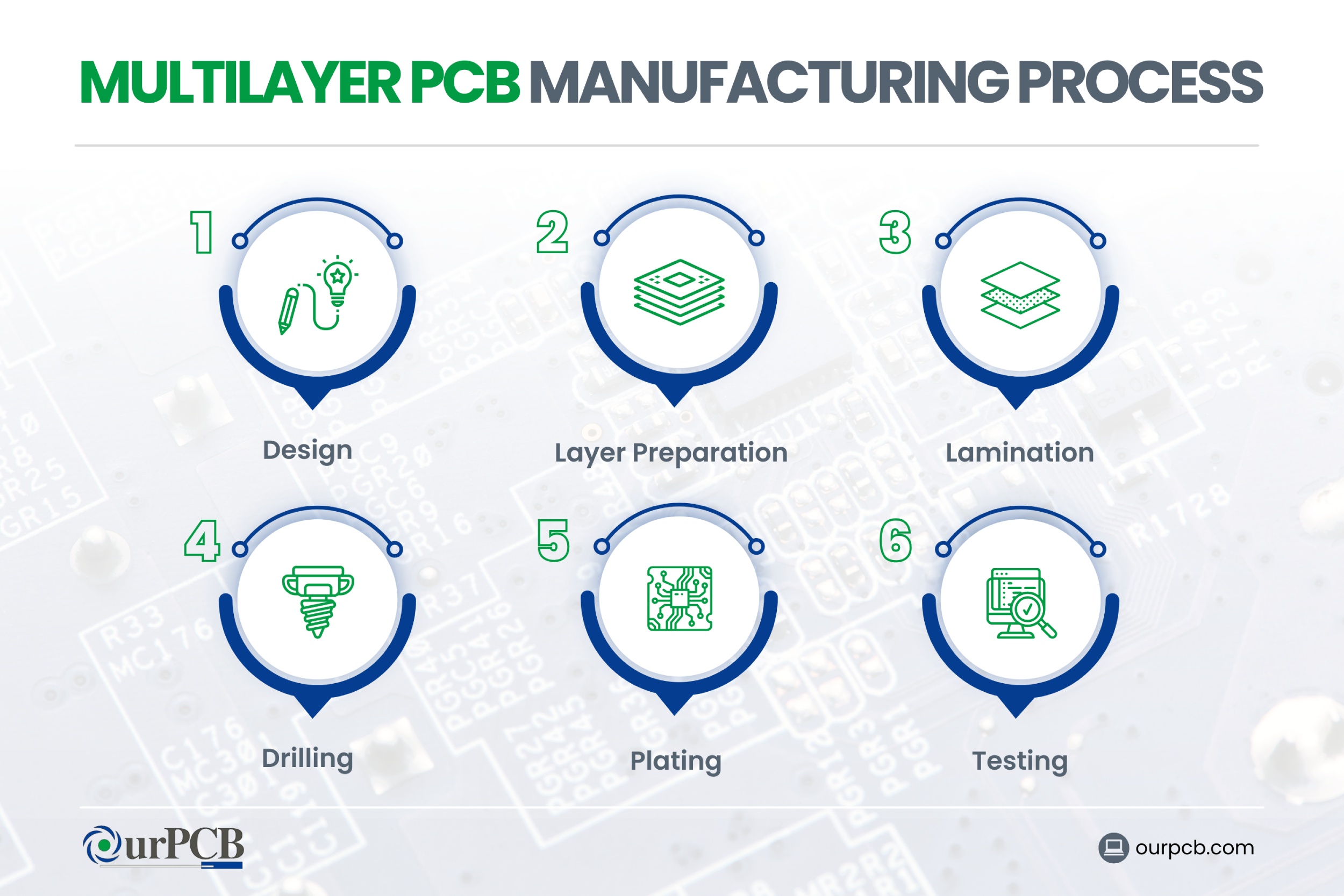
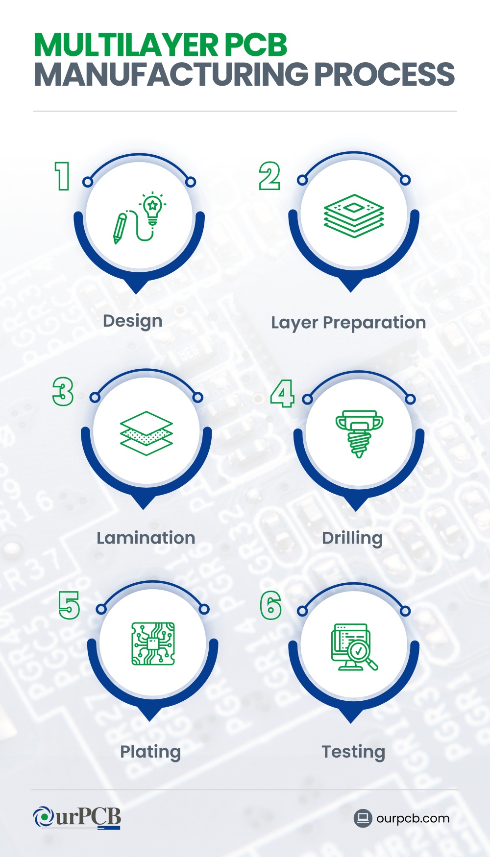
The PCB multilayer manufacturing process involves several key steps:
- Design: Engineers create a detailed PCB design using specialized software.
- Layer Preparation: Each copper layer is patterned using photolithography.
- Lamination: Layers are bonded together using heat and pressure.
- Drilling: Precision drilling creates holes for vias that connect layers.
- Plating: Vias are plated with copper to establish electrical connections.
- Testing: Each board undergoes electrical testing to ensure functionality.
Multilayer PCB Manufacturing Machines
Multilayer PCB manufacturing machines play a crucial role in production. These machines include:
- Laser Drillers: Used for precision drilling of vias
- Etching Machines: Remove unwanted copper from the board surface
- Laminators: Bond multiple layers under heat and pressure
- Plating Equipment: Apply copper to drilled vias
These machines ensure accuracy and efficiency throughout the manufacturing process.
Benefits of Multilayer Circuit Boards
Multilayer circuit boards offer several advantages, including space efficiency, design flexibility, improved performance, and more:
- Space Efficiency: They provide compact designs that save space in devices.
- Improved Performance: Reduced interference leads to better signal integrity.
- Design Flexibility: Engineers can create complex circuits tailored to specific needs.
- Higher Component Density: More components can fit within the same area compared to single-sided or double-sided PCBs.
What is a PCB Via?
A PCB via is a small hole that connects different layers of a multilayer PCB. Vias allow electrical signals to pass between these layers. They play a vital role in ensuring connectivity throughout the board.
| Type of PCB Via | Description |
|---|---|
| PCB Via | A small hole that connects different layers of a multilayer PCB, allowing electrical signals to pass. |
| Blind Hole Via | Connects an outer layer to one or more inner layers without going through the entire board. Maintains outer layer integrity. |
| Through Hole Via | Extends from the top layer to the bottom layer, providing direct connections between all layers. Suitable for various applications. |
| Buried Via | Connects only inner layers and does not appear on outer surfaces, reducing clutter while maintaining connectivity. |
Blind Hole Via
A blind hole via connects an outer layer to one or more inner layers but does not go through the entire board. This type of via helps maintain the integrity of the outer layer. It also allows connections to inner circuits.
Through Hole Via
A through hole via extends from the top layer to the bottom layer of the PCB. It provides a direct connection between all layers of the board. This makes it suitable for various applications.
Buried Via
A buried via connects only inner layers and does not appear on the outer surfaces of the PCB. This type of via helps reduce clutter on the outer layers while maintaining connectivity between inner circuits.
OurPCB: High-Quality Multilayer Boards
OurPCB offers high-quality multilayer boards designed for various applications. We provide reliable solutions tailored to your needs. Explore our range of products today, including multilayer PCBs. Contact us for your next project!
FAQs on What is a Multilayer PCB?
What is the difference between single and multilayer PCB?
Single and double-sided PCBs have fewer layers and simpler designs compared to multilayer PCBs. Multilayer PCBs incorporate multiple layers of the multilayer PCB stacked together. A single or double-sided PCB is suitable for basic applications. However, multilayer PCBs are designed for complex circuits. Multilayer PCBs have advantages of multilayer PCBs like higher functionality and compact size. Advanced manufacturing techniques are required for multilayer PCB design, making them more intricate and suited for demanding tasks.
How to tell if a PCB is multilayer?
You can identify a multilayer PCB by inspecting its inner layer core and the bottom layers of the multilayer structure. This is visible in its cross-section. Multilayer PCBs provide more than one single connection point, making them distinct from simpler PCB types. Expert analysis or consulting a multilayer PCB manufacturer can confirm the number of layers and complexity.
What are the disadvantages of multilayer?
The main drawbacks of multilayer PCBs are their higher cost and the complexity of PCB assembly compared to single and double-sided PCBs. They require advanced expertise from PCB manufacturers. They can also be challenging to repair or modify. Despite the benefits of using multilayer PCBs, they are less suitable for applications where simpler types of PCBs suffice or cost efficiency is critical.
Back to Top: What is a Multilayer PCB?
Special Offer: Get $100 off your order!
Email [email protected] to get started!