In certain applications, like most wall chargers and computer power supplies, the input energy is taken from the wall outlet, which is usually 220V. It is considered a higher than usual voltage for a PCB, and often, special considerations have to be taken whenever designing a board that has a high voltage line on it.
This article will cover everything you need to know about high voltage PCBs
Contents
- 1、High Voltage PCBs and Things You Need to Know About Them
- 1.1 What is a high voltage PCB?
- 1.2 Dielectric Strength
- 1.3 Creepage Distance
- 1.4 Clearance
- 1.5 Solder Mask
- 2、 Design Practices for High Voltage PCBs
- 2.1 Routing
- 2.2 Polygon Planes
- 2.3 Internal Layers
- 2.4 EMI Considerations
- 3、Component Selection
- 3.1 High-Frequency Transformers
- 3.2 Mosfets/Transistors/Switches
- 3.3 Passive Components
- 4、Special Board Features
- 4.1 Isolation Slots and cut-outs
- 4.2 Board Material
- 4.3 Board Finishing
- 5、What OurPCB Offers
- Quick turnaround time
- Wide variety of options
- Online Quotation System
- 6、Conclusion
1、High Voltage PCBs and Things You Need to Know About Them
1.1 What is a high voltage PCB?
In short, any PCB that runs at a much higher voltage than the normal rail voltage can call a medium or high voltage PCB. Boards like mains powered power supplies, Inverters, EV chargers, etc. fall into this category.
There is no fixed number over which board would be considered high voltage. But as a rule of thumb, you could consider something like 100V, beyond which you would want to take special design rules into account.
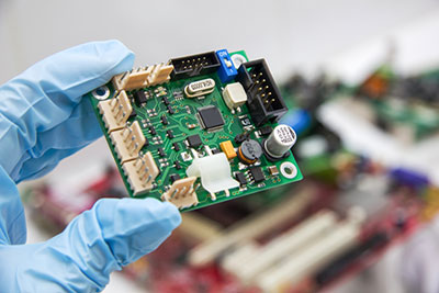
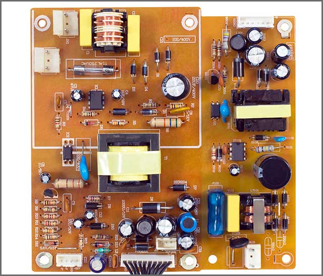 Image 1: A mains voltage switched-mode power supply
1.2 Dielectric Strength
The dielectric strength of a material is the maximum electric field the material can withstand without losing its insulating properties.
Usually, this would be FR4 for most PCBs.
So the first important thing to check is the dielectric strength of your PCB material.
FR4 rated for 300 mils/mil; however, IPC standards will recommend a spacing of 3.9mils for 80V.
It is often wise to leave room for it and therefore follow IPC standards.
1.3 Creepage Distance
Creepage distance is the shortest distance between two conductive parts along the surface of a solid insulating material.
The main basis for the determination of creepage distance is the long-term voltage applied on the two conductors. Over time, there can be contamination on the board, so it is wise to have additional headroom.
Creepage distance recommendations for most components and layouts are usually provided in their datasheets. It is one of the important parameters when it comes to High Voltage PCBs.
1.4 Clearance
Clearance is the shortest distance in air between two conductive parts. The dielectric strength of the air governs the clearance. Air usually breaks down at about 3KV per mm. However, under conditions of moisture and contamination, this value can go much lower. The IPC standards specify different clearance distances for design types.
Most components are already compliant, and they are packaged in packages of high enough pin pitch.
For example, a 600V rated Mosfet will usually come in a TO-220 or TO-247 package.
More information about creepage and clearance can be found here:

1.5 Solder Mask
The solder mask also acts as an insulator to some extent. So for boards with very fine pin pitch and high voltage between pins. It is important to go with a manufacturer who can apply a solder mask between PCB's the fine pitch PCB.
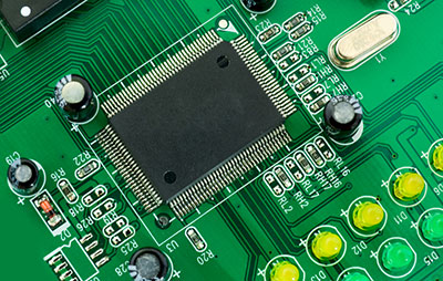
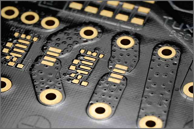 Image 2: A PCB with black solder mask
2、 Design Practices for High Voltage PCBs
2.1 Routing
Whenever routing traces for high voltage PCBs, the following points are most important:
1.Keeping clearance between traces that have a high voltage difference between them.
2.Avoiding any sharp turns and edges as these can act as areas of the concentrated electric field.
3.Avoid running very high voltage traces on the internal layers of the board.
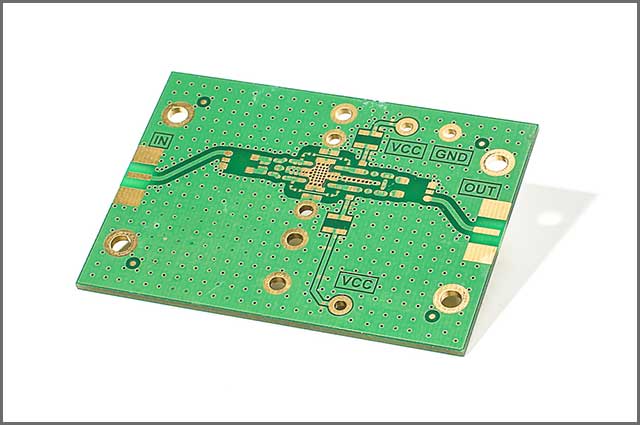 Image 3: A PCB with larger than usual plane clearance
2.2 Polygon Planes
For all high voltage PCBs, the polygon plane clearance should be increased to a safe value and certain sections of the board.
For example, if there is a trace carrying 600V towards an edge connector on a board, then a lot of times, the design won't have a polygon pour near that trace.
Also, internal planes on a multi-layer PCB should not have a very high voltage or a very small distance between them.
2.3 Internal Layers
It is possible to make multi-layers with the medium voltage on all layers. The major consideration is the proper filling of the spaces between the layers. The thickness of the separation between layers must be at least .005" to maintain the filling medium's integrity, prepreg. Any voids or pockets will degrade the dielectric value seriously.
The standard prepreg FR4 type multi-layer is not suited to medium or high voltage work. The material breaks down too fast and does not feature a homogeneous internal structure. The excess microvoids degrade the dielectric rating resulting in its poor performance.
2.4 EMI Considerations
High voltage PCBs are notorious for emitting disturbances over a wide spectrum.
The most important thing to minimize these is to have a small loop area and extensive via stitching to the ground plane wherever possible.
Additionally, the high voltage components can also be potted and then shielded by a metallic sheet.
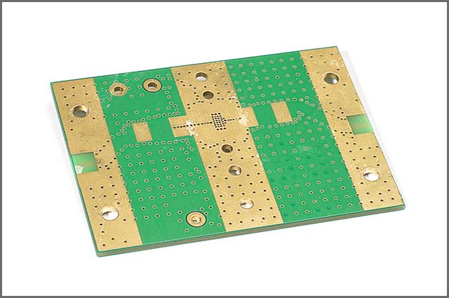 Image 4: Aboard with extensive via stitching
Special Offer: Get $100 off your order!
Email [email protected] to get started!
3、Component Selection
3.1 High-Frequency Transformers
Most high voltage boards will almost always involve a switch-mode circuit with a transformer to produce the high voltage. In these cases, you must comply with the core insulation level of the transformer.
Regarding the PCB layout, the ground plane should ideally separate between the primary side and the secondary side. There should be a large isolation gap with cut-outs on the board between the primary and secondary sides.
3.2 Mosfets/Transistors/Switches
Most of the time, the high voltage devices will come in the correct package rated to withstand the high voltage between pitch.
Even then, it is a good practice to pick the device with the largest pin pitch if you know the voltages would be quite high. A common example will be to pick a TO-247 device instead of a TO-220 if there are no space constraints. Similar examples can be applied for SMD devices as well.
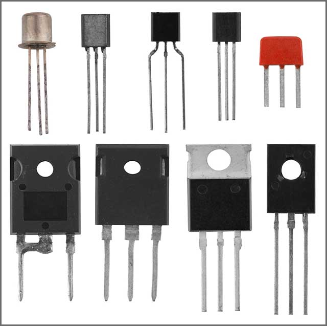 Image 5: Transistors in different packages
3.3 Passive Components
When picking passive components, the component size is crucial as it is directly dependant on the voltage it can tolerate. So let's say the design has 300V between an SMD resistor. Then it would be much better to choose a package like 1206 rather than 0402. It is often a requirement to put multiple such components in series to reduce voltage stress across them
4、Special Board Features
4.1 Isolation Slots and cut-outs
Most high voltage boards require isolation slots and board cut-outs near any board section, which carries high voltage.
In many consumer devices like chargers and power supplies, these slots and board cut-outs are mandatory to pass certain safety standards. These features add an extra layer of safety and would help in high humidity environments and cases where contamination is likely.
Isolation slots and cut-outs will usually have to define on a mechanical layer of the board.
4.2 Board Material
Standard FR-4 is not a good material for high voltage boards as it has low dielectric strength.
Whenever the cost is not a constraint, it is better to go for a board material with a higher dielectric strength. Some of the high voltage rated materials are:
1.BT Epoxy
2.Polyimide
3.Isola
4.3 Board Finishing
The most underlooked and important factor when it comes to high voltage PCBs is the board finishing. It mainly includes the surface finish on the pads and any exposed traces. Mainly the finished board should have a smooth finish free of any bumps and should be even along the entire surface.
Any imperfections on the high voltage pads like sharp points can result in a high electric field region, which can then cause arcing.
5、What OurPCB Offers
Quick turnaround time
We have a super quick turnaround time of only 24hours for two-layer boards and just 48hours for four-layer boards. It is one of the most important factors for engineering teams who quickly test out prototype boards.
Wide variety of options
For board manufacturing, OurPCB has a wide selection of different parameters. It includes the type of PCB material you want to use, the surface finish along with options for adding unique identifiers for your boards.
OurPCB can also manufacture boards up to 32 Layers.
Online Quotation System
Finally, OurPCB also has an online quotation system that automatically calculates the price of your PCB after you upload your Gerber files and input the required data.
6、Conclusion
A high voltage PCB is something that needs precision in both the board layout and manufacturing stages. If you follow all the rules and general practices for high-pressure rules, then getting a working board that will last a long time is easily within reach.
OurPCB offers the perfect balance between price and quality and a variety of manufacturing options that may be suitable for high voltage boards.
For more information, contact OurPCB via their website:
Special Offer: Get $100 off your order!
Email [email protected] to get started!