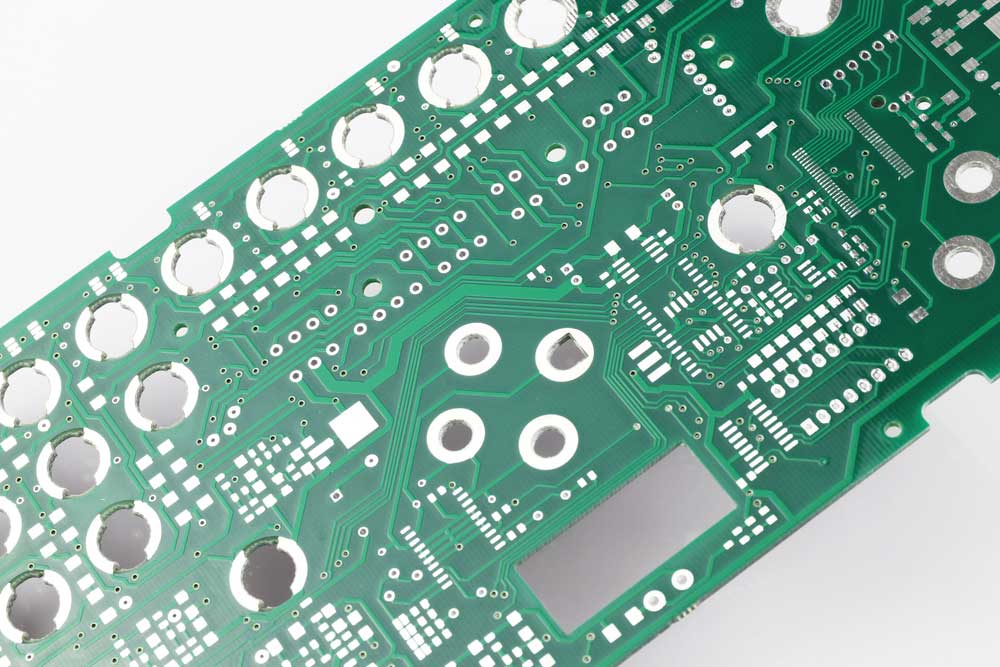
In the PCB manufacturing world, you may have come across the terminologies blind via and buried via. As highlighted in most of our PCB articles and other DIY blogs in general, components have become progressively refined. Besides, lesser form factor gadgets are dominating most electronic products manufactured today.
The need to link components to the two sides of these complex printed circuit boards should be among your priorities when designing a PCB. Basically, you require blind and buried vias to connect components to various sides of your PCB. For a comprehensive overview, this article takes a deep dive into the different vias available, the uses, advantages, and disadvantages, as well as how to get an accurate PCB quotation online.
Contents
- Types of Blind Vias
- Photo-Defined Blind Via PCB
- Sequential Lamination Blind Via
- Controlled Depth Drilled Vias
- Laser Drilled Blind Vias
- How do Blind Via PCB Compare with Buried Via PCB?
- Blind Via PCB: Pros and Cons
- Pros
- Cons
- Blind Via PCB Applications
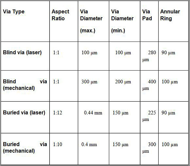
- Blind Via PCB Aspect Ratio
- How to Make Blind Via PCB
- Blind Via Cost
- Conclusion
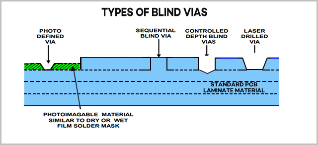
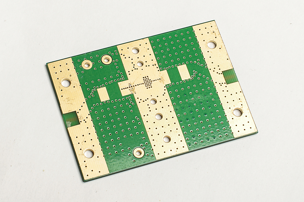
Types of Blind Vias
There are four categories of blind vias for your information, and we will discuss each of them in detail here. The diagram below shows the different types of PCB vias.
-
Photo-Defined Blind Via PCB
You can make a photo-defined blind by coating a photo-reactive resin sheet to a core. The core should consist of laminated traces enriched with planes and submerged signal layers. Remember to cover your photo-reactive sheet with patterns that shield the points where you will make the holes. You should also expose the sheet to wavelength rays to harden the residues on the board. After that, immerse your circuit board in a dying mixture to eliminate any unwanted substance from the holes. When you have finished the scraping process, plate copper into the holes and on the surfaces to form the board's surface layer.
-
Sequential Lamination Blind Via
You can make this type of blind vias by passing a thin laminate piece through the two-faced PCB process. First, you need to drill, coat, and sketch the laminate to outline the characteristics that will make your PCB's second layer. Leave the solid copper material on the other PCB part to act as your board's first layer. It would be best if you also laminated your subassembly with the different board layers. For a seamless design, choosing high-quality PCB materials for manufacturing is important to ensure durability and functionality in multilayer boards. Finally, pass your product through the process of making the surface layers of a multilayer board.
-
Controlled Depth Drilled Vias
As illustrated in figure 1, you can make controlled-depth vias using the through-hole via approach. However, you should set your drill to pierce only halfway through the board. This precise technique relies heavily on the accuracy and methods involved in PCB drill processes to ensure the proper depth and functionality. You also need to place a pad on the second layer so that the drill penetrates it. Besides, it would help if you were cautious to ensure there are components underneath the percolated hole, forming contact with it. Lastly, you need to coat copper in the percolated hole concurrently with plating copper in the through-hole blind vias.
-
Laser Drilled Blind Vias
You can create these vias after laminating all your board layers; you can create these vias before designing and coating the surface layer. Use a laser to remove the copper on the surface layer and the insulating substance between the first and second layers. Remember, you can either use the CO2 or Excimer laser.
How do Blind Via PCB Compare with Buried Via PCB?
Blind Via PCB: Pros and Cons
Pros
The better utilization rate of surface space for top and bottom mounted components.
They present minimal interferences between signals, which is vital for maintaining signal integrity in high-performance circuit designs.
Blind vias present better pad density and wiring compared to standard boards.
Cons
The blind vias production process has higher demands.
They have a complex manufacturing cycle.
Lastly, they are expensive to produce due to extra processes and equipment.
Special Offer: Get $100 off your order!
Email [email protected] to get started!
Blind Via PCB Applications
This part will take a closer look at the two primary uses of blind vias in circuit boards. It is essential to realize that you can minimize your circuit board layers by expanding the ball-grid getaway channel. You can achieve that by creating blind vias.
Are you experiencing difficulties when penetrating through-hole vias for designing and trace breakout of BGA? If so, try increasing the getaway channels on the internal and lower layers with blind vias. Alternatively, you can use blind vias to reduce your circuit board aspect ratio.
Mostly, circuit board BGA components come with various pitches. For example, a 4.00mm radius board contains 0.8mm and 1.27mm pitch BGAs. Remember, the smallest size via hole is determined by both the drill and board aspect ratios.
Blind Via PCB Aspect Ratio
You can calculate the blind via aspect ratio as shown below:
PCB Aspect ratio = PCB Thickness divided by the Diameter of the Drilled Hole.
Note that blind vias will minimize your board aspect ratio by decreasing the number of supported layers. Therefore, use blind-hole vias instead of through-hole.
How to Make Blind Via PCB
Circuit boards with blind vias use the necessary procedure of creating multilayer boards up to the drilling step. As mentioned earlier, blind vias provide more holes that facilitate connections between two layers for two-layered boards. Designing an effective PCB stackup is essential during the planning phase to ensure proper layer alignment and accommodate the blind vias. Choose your build-up and contact your manufacturer before you start the circuit board design process.
It is important to note that you may encounter problems if you try adding vias 'on the go.' Mostly, you will run short of space, and most probably, you may abandon the PCB and start creating afresh. That is a waste of your precious time and resources. Therefore, follow the steps below keenly to avoid making mistakes.
But before that, let us look at the rules of blind vias:
- Blind vias start from either the upper or lower layers of the board.
- It would help if you placed them on the layers evenly.
- Blind vias should not percolate the entire PCB.
- They should not start or end in the middle of the board substrate.
The hole height and hole diameter (H/d) value should be less than one. Actually, 0.8 is the best value. That means you should assign big diameters to deep vias. Furthermore, huge vias also require significant dielectric gaps.
To accurately create a blind via, you need to drill the vias within the central cores. Afterward, let the vias reach the outside layers. Lastly, prepreg to stack together with the layers.
Blind Via Cost
Since you drill through just some layers when making blind vias, you will make holes and coat them before combining the PCB layers. That calls for extra lamination processes compared to the single lamination needed in through-hole vias. These additional processes consume more time and resources, making the blind vias production process costly. But, the advantages of blind vias offset the extra cost in many instances.
Conclusion
Are you considering applying blind vias in your circuit board design? We encourage you to go ahead with your plans and take advantage of the numerous benefits of blind vias. This article has unearthed almost everything you should know about circuit board blind vias. It has touched on the different blind vias available to the applications to the advantages and disadvantages of blind vias.
We have rich experience in designing and manufacturing PCB blind vias. Regardless of your unique needs, we can produce products tailored to your specific needs.
Back to Top: Blind Vias PCB
Special Offer: Get $100 off your order!
Email [email protected] to get started!