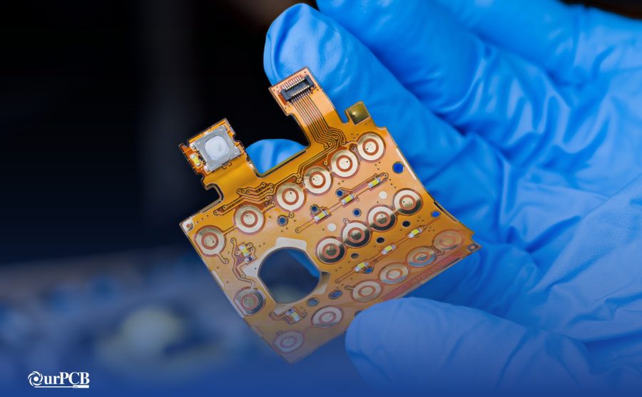
Circuit tests are an integral part of the PCB assembly service process. Running functional tests can help manufacturers ensure product quality and prevent a wide range of manufacturing defects. However, they need to understand what PCBA test they have at their disposal. Thus, the following guide will explore the intricacies of PCBA testing and why it's so important. But first, let's explore what a PCBA test is. To get an accurate estimate for your needs, consider requesting an online pcb quote.
Contents
- What is PCBA Testing?
- Benefits of PCBA Testing
- Most Popular PCBA Testing Methods
- Visual Inspection
- In-circuit testing (ICT/Bed of nails)
- Flying Probe Testing (FPT)
- Automated Optical Inspection (AOI)
- Automated X-ray Inspection (AXI)
- Burn-in Testing:
- Functional testing (FCT)
- Fatigue Test
- Aging Test
- PCBA Test Equipment
- Common Defects found in PCBA testing
- The Future of PCBA Testing Technology
What is PCBA Testing?
The PCBA process involves operating a set of disparate and complex equipment. If there is an error in any equipment or how workers use it, it may fault the final product. Some of these faults are easy to detect, while others are more subtle.
Thus, we require different techniques to detect these faults. Some of the most common PCBA tests include in-circuit tests (ICT), functional circuit tests (FCT), burn-in tests, and fatigue tests. Are you in need of top-notch PCBA services with reliable PCBA testing methods? We at OurPCB are ready to assist you.
Benefits of PCBA Testing
An inspector holding a PCB after optical inspection
PCBA testing allows us to detect any fatal errors before mass-producing the PCB. It enables companies and manufacturers to save time and money and avoid any brand identity or reputation threat. As such, the sooner manufacturers can detect defects in the PCBA process, the easier and cheaper it will be to rectify them.
Special Offer: Get $100 off your order!
Email [email protected] to get started!
Most Popular PCBA Testing Methods
The most popular PCBA testing procedures are:
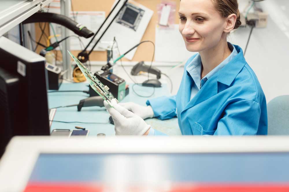
Visual Inspection
An operator visually inspects a PCB assembly.
This technique involves an experienced technician manually inspecting the PCB through their naked eyes or magnifiers. It's cheap, and we can easily find most PCB soldering problems using this method. However, detection largely depends on the technician's skill. Additionally, you can only inspect visible solder joints. Thus, it may be more suitable for smaller productions with simple PCBA designs.
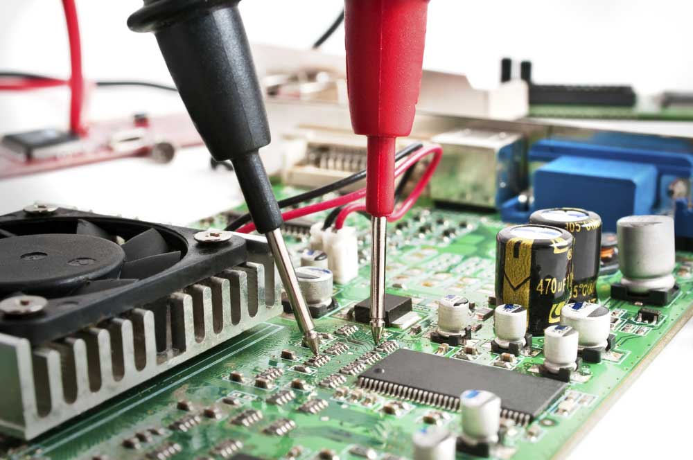
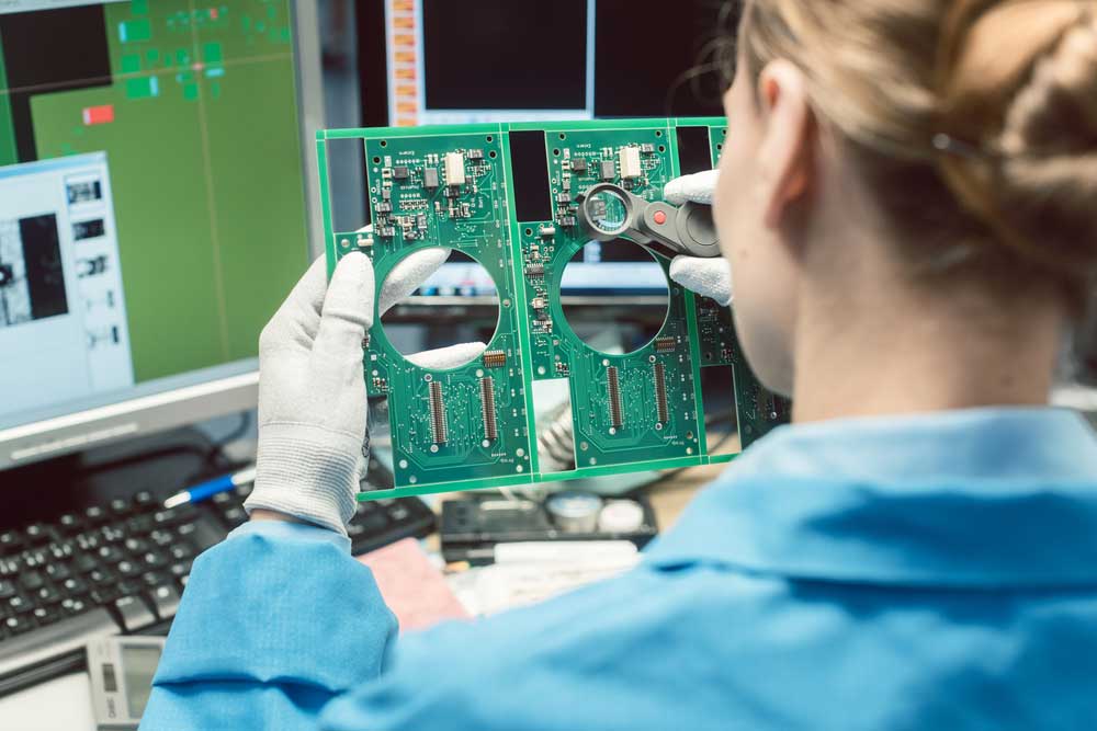
In-circuit testing (ICT/Bed of nails)
Engineers running PCBA test
A software-operated process where a machine (or operator) places the PCB on a set of spring-loaded pins. The pins align to different testing points on the PCB. People often refer to this method as the bed of nails test because of how the plugs look. It can detect any faults such as shorts or opens. Additionally, it can test the resistance and capacitance to ensure that the PCB's' final specifications are accurate. In-circuit testing may be expensive because PCBs with different designs require other fixtures.
Flying Probe Testing (FPT)
This technique is a less expensive alternative to in-circuit testing, where a set of high-precision mobile needles/pins hover above a PCB. These pins will probe into software-specified regions of the PCB. Flying probe tests are more versatile because they don't require fixtures. This testing technique has a few benefits, and the price is one of them.
Automated Optical Inspection (AOI)
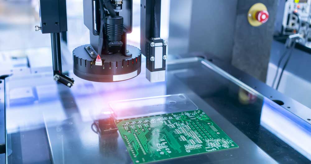
Vision measuring instrument inspecting a PCB Circuit
Manufacturers typically perform this test before and after the wave soldering or reflow process. However, some companies may perform AOI testing in various stages of production. In this process, the manufacturer employs a high-resolution camera to scan the PCB's surface for defects.
Automated X-ray Inspection (AXI)
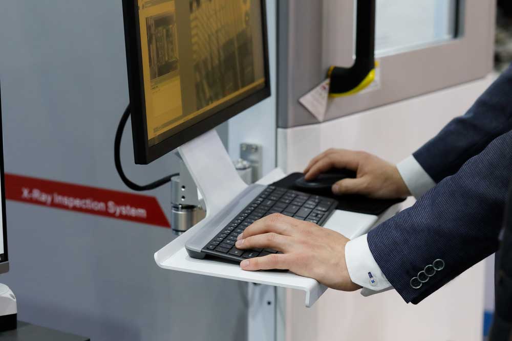
An operator checking the X-ray of a printed circuit board
AXI is a process where manufacturers use X-ray imaging to reveal hidden defects in the PCB. It uncovers faults that we cannot tell. For instance, it may help detect subtle errors in alignment, nano breaks in the soldering, etc. It's' particularly suitable for ball grid arrays and chip-scale packages where the solder joints aren't' visible to optical techniques. Typically, automated x-ray inspection can ensure the long-term quality of solder joints and connections. Additionally, this method seems to have the highest detection rates of nearly any inspection method.
Burn-in Testing:
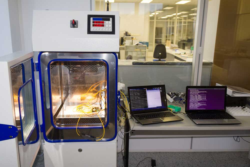
Opened temperature and climate test chamber for PCBs and electronic components
This method involves stress testing the PCB under extreme conditions. For instance, it may include running the PCB under extreme temperatures, high voltages, etc. This testing technique helps engineers identify errors in the PCBA's' operation. However, it may be labor-intense extremely time-consuming. Furthermore, it may shorten the PCB's' lifespan. However, it ensures its reliability.
Functional testing (FCT)
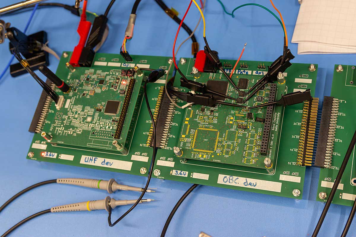
Foresail-1 Flatsat PCBs
Source: Wikimedia Commons
A varied PCBA testing technique involves testing the board by simulating its operating environment. Manufacturers perform this test in the last phase of the production cycle. It doesn't require any specialized equipment in most cases, making it cheaper.
Nevertheless, the effectiveness of the detection depends on the test plan. Experienced technicians will need to isolate and identify the cause of any faults they detect during the test. Additionally, a functional test is not a stress test. Thus, the PCB may still fail if it operates under extreme conditions.
Fatigue Test
In this type of test, an operator will take a sample of the PCB assembly and conduct a high-frequency test until the board fails. Of course, this test can be time-consuming, as some boards may take a very long time to reach failure. Nevertheless, manufacturers generally use this method after a failure occurs in their products. It helps them troubleshoot and fix these faults.
Aging Test
PCB with corrosion as result of Aging PCB Test
Source: Wikimedia Commons
This technique is similar to the fatigue test. A quality assurance specialist will operate or power the PCB for a set time (or until it fails). The specialist will measure or detect any faults or failures in the PCBA's operation during this period. While it is time-consuming, it's highly effective in ensuring the final product's quality.
PCBA Test Equipment
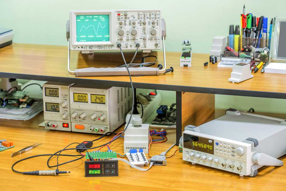
Electronic workshop and testing Equipment
Each PCB test technique requires its own set of tools and test equipment. Some of the most common PCBA test equipment and systems include:
- In-circuit test machines
- Flying probe machines
- Workbenches with magnifiers
- Automated optical inspection machines and systems
- Automatic x-ray inspection machines and systems
- Ovens and climate/weather simulation chambers
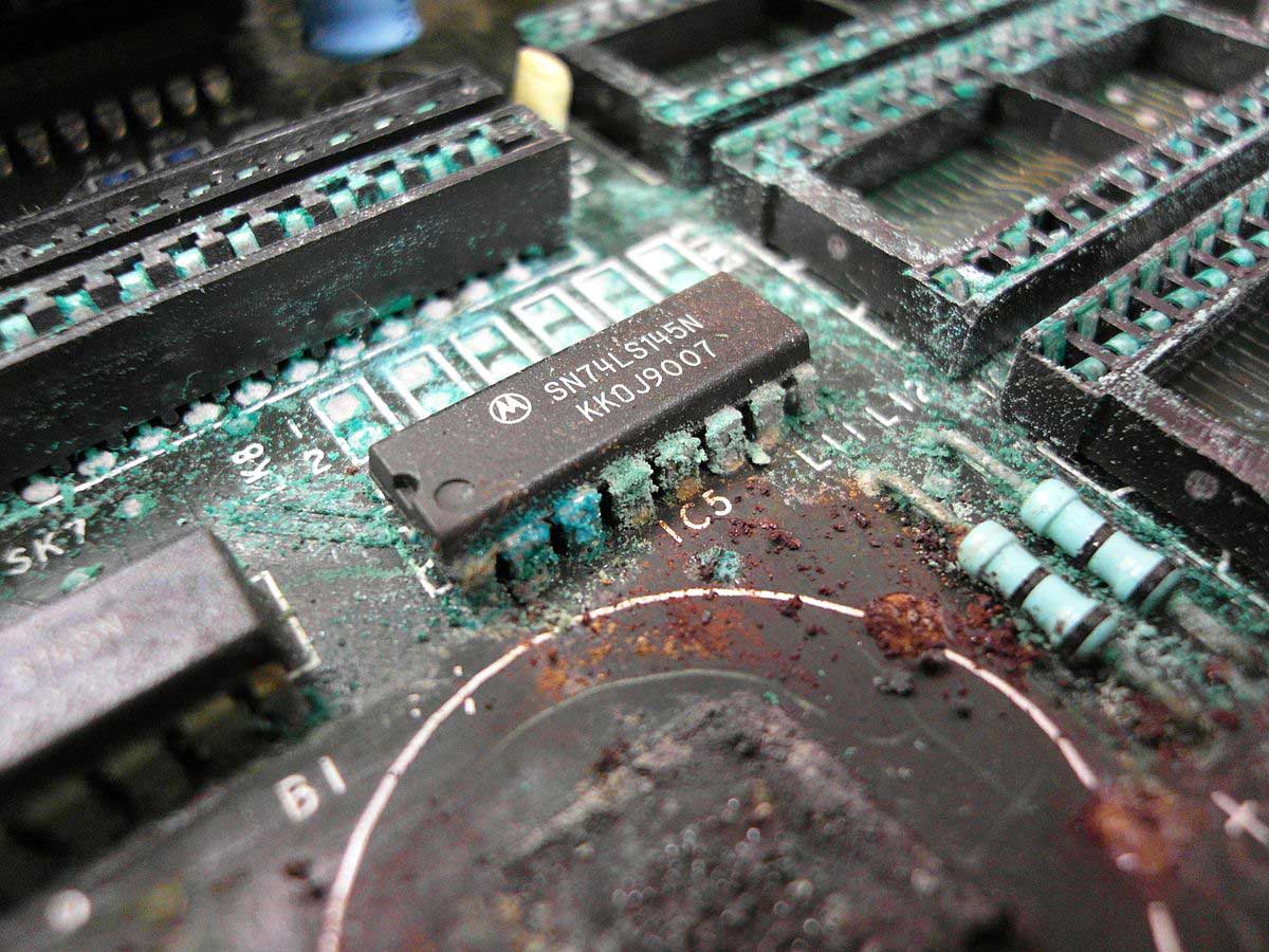
Common Defects found in PCBA testing
Some common defects that a PCBA test may detect include:
- Tombstoning: Occurs when a passive SMT component (such as a resistor) lifts from one end, resembling a tombstone in a graveyard.
- Opens: Refers to open solder joints that occur when leads and pads fail to bond correctly.
- Missing and damaged components: Some components may be missing or damaged due to manufacturing errors.
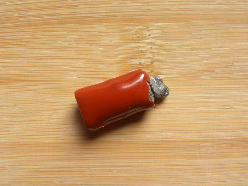
Damaged red ceramic capacitor
- Too much solder: Large blots of solder could form around the joints, causing future problems. Additionally, it is inefficient and messy.
- Solder bridges: Occurs when solder erroneously connects one lead to another lead. It may cause components to be short or burn up. Additionally, it may potentially cause the PCB trace to burn out.
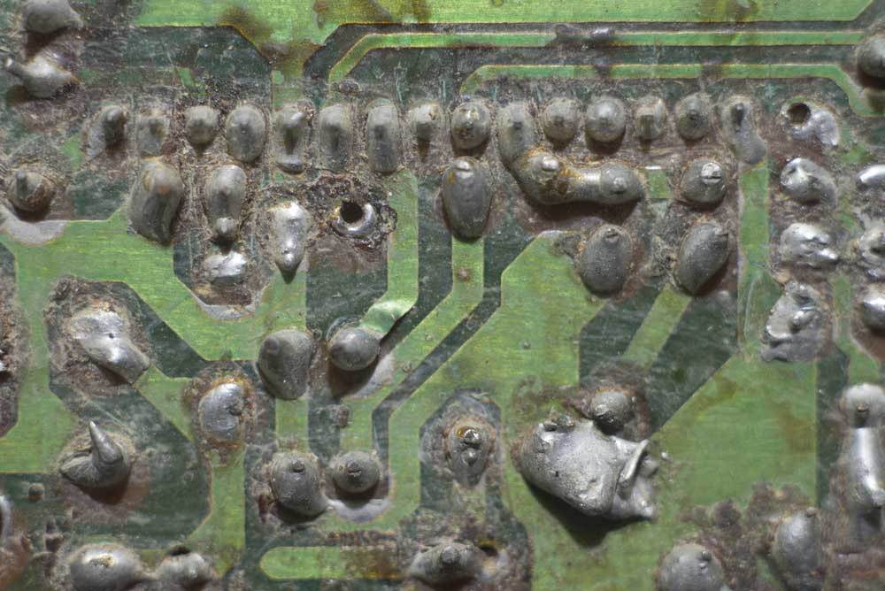 Closeup of a damaged circuit board found during PCBA testing
- Webbing and splashes: Occur when contaminants contact the PCB during the soldering or product development. Not only do they interfere with the appearance of the PCB, but they may also cause short-circuits and other issues.
- Lifted pads: When there is too little solder on the pads, they may start to lift. If we apply force to them, this situation may ultimately cause component failures or a short circuit that may inevitably destroy the PCB.
The Future of PCBA Testing Technology

Engineer & Designer running a PCBA testing
The complexity of PCBA fabrication will determine the future of its test technology. Furthermore, artificial intelligence will have a tremendous influence on it too. It will increase automation and accuracy while rendering the need for human operators unnecessary. Additionally, it will cut down on testing times because machines and computers will require less programming. It is the future of PCBA testing and the entire PCB assembly service process.
You can judge how reliable a pcb maker is by what PCBA testing techniques and technology they implement in their factories. The more multi-faceted their test approaches are, the lesser final product defects. As the above guide illustrates, PCBA testing is essential and significantly impacts a PCB's quality. Thus, you should always invest in a pcb maker with thorough PCBA testing.
Back to top: What is PCBA Testing?
Special Offer: Get $100 off your order!
Email [email protected] to get started!