SWD is a two-pin ARM-specific serial debugging interface that replaces the 5-pin parallel JTAG interface to communicate with microcontroller devices.
So SWD programming uses the SWDIO (bi-directional data line) and SWCLK (host-driven clock line) pins to send/receive data from a microcontroller.
The interface has a third optional output pin (SWO) that is asynchronous to the other debug pins but is unavailable on most SWD-supporting devices.
Let’s look at SWD programming by covering its communication protocol, data reading/writing from SRAM register addresses, and programming the SRAM over SWD.
Contents
- SWD Implementation
- SWD Interface Communication Protocol
- Successful Connection and Line Resetting
- Successful Transaction
- Turnaround Period
- Registers Used for SWD Serial Communication
- Debug Port Registers
- Memory Access Port (MEM-AP) Registers
- Debug and System Registers
- SRAM Programming
- Memory Access Source Code
- Core Register Access Source Code
- SRAM Firmware Programming
- Wrap Up
SWD Implementation
As stated earlier, SWD (Serial Wire Debug) is a 2-pin JTAG alternative. But it has the same JTAG protocol on top and uses ARM’s bi-directional wire protocol CPU standard as defined in the organization’s debug interface v5.
Therefore, you can use SWD as an AMBA bus master to debug registers and access memory from peripheral devices or the internal system.
The two pins only form the physical connection. Past that, you go into the debug interface v5, which contains the debug access port.
This port has two control units. The first is the debug port, which links directly to the two pins (physical connection). It is vital to note that the two pins are part of the DP.

ARM’s debug interface implementation with the 2-pin SWD physical connection to external devices
So, external devices communicate with the debug port over SWDIO and SWCLK.
This port can then access one or several access ports, which form the second control unit.
As the name suggests, these access ports give access to the rest of the system.
The most vital access port is the memory AP because it provides access to all the peripheral and memory registers in the internal APB or AHB buses.
Special Offer: Get $100 off your order!
Email [email protected] to get started!
SWD Interface Communication Protocol
The SWD interface can have three operations. These include successful connection, line reset, and successful transaction.
Successful Connection and Line Resetting
The DP uses 50 clock cycles where the data input is 1 for the connection sequence. This same sequence helps with line resetting.
For JTAG to SWD switching, the combined direct port for both protocols (SWJ-DP) implements a watcher circuit to detect a unique 16-bit selection sequence on the SWDIOTMS pin.
This 16-bit sequence can either have the Most Significant Bit (MSB) or Least Significant Bit (LSB) first. If MSB first, the SWD sequence is 16’h79E7. But if LSB first, it is 16’hE779E.
After reading this line request sequence, the host must read the IDCODE register for confirmation that the packet frame alignment is correct and received.
A pallet of microcontrollers
SRAM Programming (Initialization)
Considering the connection and line reset steps above, the DP initialization sequence follows this procedure to bring it to a “know” state.
- Send over 50 SWCLKTCK clock cycles where the SWDIOTMS data input is 1 to put JTAG and SWD in their reset states.
- Transmit the 16-bit JTAG-to-SWD selection sequence on SWDIOTMS.
- Repeat step 1 to ensure SWD goes into “line reset” mode if SWJ-DP was in SWD mode before transmitting the selection sequence.
- Do a READID to check if SWJ-DP has shifted to SWD mode.
Successful Transaction
The transaction process must go through these three phases for it to be successful.
Packet Request Phase
The host device sends an 8-bit write packet request to the target board, where the bits have these meanings.
- A start bit with a value of 1
- An APnDP single bit to show whether to access the access or debug port (1 for accessing the AP and 0 for the DP)
- A single RnW bit, where 0 implies “write access” and 1 indicates “read access.”
- Two A[2:3] bits give the address field for the AP or DP register address.
- A parity bit over the APnDP, RnW, and A[2:3] bits, which gets set to 1 if there is an odd number of bits in the 8-bit sequence set to 1 (otherwise, it will be a zero)
- One stop bit
- A park bit with a value of one
ACK Phase (Acknowledge Response)
After receiving the packet request, the target board responds with a 3-bit LSB first OKAY acknowledgment. These bits have the following meanings.
- OK indicates a successful operation if the value is b001
- WAIT has the value b010 (indicates the host should retry the sending operation later)
- FAULT indicates an error occurrence using the value b100 and sets a sticky bit in STAT or CTRL.
The host can identify the error by checking the sticky error bits and must clear the ABORT register before using AP commands.
Data Transfer Phase
The final phase is data transfer, where the host or target device sends a 33-bit data phase (32 bits of data and a parity bit), depending on whether it is a read or write operation.
The parity bit operates like the one in the packet request.
Turnaround Period
A turnaround period occurs between the three phases above when the SWDIO pin changes direction. This period is a single clock cycle, and the two sides ignore it because it contains zero bits.
Registers Used for SWD Serial Communication
This serial communication uses debug port (DP), memory access port (MEM-AP), debug, and system registers.
Debug Port Registers
These SW-DP registers can differ depending on whether it is a read or write operation.
| Address | Read | Write |
| 0x00 | IDCODE | ABORT |
| 0x04 | CTRL/STAT | CTRL/STAT |
| 0x08 | RESEND | SELECT |
| 0x0C | RDBUFF | N/A |
Memory Access Port (MEM-AP) Registers
MEM-AP registers give the Debug Access Port access to the memory in the microprocessor core.
So, you can use them to program and debug Cortex M3 processors because the peripherals, memory, and debug components map to the memory.
You can use the following addresses for the debugging and programming functions.
| Address | Bank | Function/Description | |
| 0x00 | 0x00 | CSW (Control/Status Word Register) | |
| 0x04 | 0x00 | TAR (Transfer Address Register) | |
| 0x0C | 0x00 | DRW (Data Read/Write Register) | |
| 0xFC | 0x0F | IDR (Identification Register) | |
Debug and System Registers
There are five debug and system registers that you can use to set the processor’s core halt mode to put it and its connected peripherals into a “know” state.
This mode also stops the processor from running partial code accidentally when writing the program.
You can also use these registers to alter the core addresses like PC and SP. They include the following.
| Address | Name | Description/Function |
| 0xE000EDF0 | DHCSR | Debug Halting Control & Status Register |
| 0xE000EDF4 | DCRSR | Debug Core Register Selector Register |
| 0xE000EDF8 | DCRDR | Debug Core Register Data Register |
| 0xE000EDFC | DEMCR | Debug Exception & Monitor Control Register |
| 0xE000ED0C | AIRCR | Application Interrupt & Reset Control Register |
If you have the Silabs SiM3U167 microcontroller unit, you can use a Python script to implement a high-level protocol to halt its core via the debug and system registers.
The halting process is as follows.
- Begin by writing 0x08 to the Silabs extent AP register CHIPAP_CTRL1
- Write 0xA05F0001 to register DHCSR to enable the halting debug register
- Enable DEMCR by writing it to 0x01, which activates the reset vector catch
- Reset the core by writing AIRCR to 0xFA050004
- Write CHIPAP-CTRL1 to 0x00
SRAM Programming
The high-level Python script for the Silabs SiM3U167 calls the Silabs DLL interface, enabling it to access the USB debug adapter.
So here are some Python script examples for programming the internal SRAM over SWD.
Memory Access Source Code
This code sets a 32-bit width with auto increment in the CSW register, writes the memory address in the TAR register, then accesses the DRW register to read or write the data.

Core Register Access Source Code
This software code is similar to the one above because it implements write and read functions. The former does these tasks.
- Set the CSW register to a 32-bit width
- Write the address of the DCRDR into the TAR register
- Write the core value in the DRW register
- Repeat step two
- Write REGWnR=1 and the core register index Rn into the DRW register
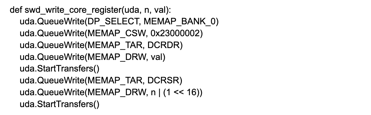
The read function is similar to the write procedure because it begins with setting a 32-bit width and writing the DCRDR address into the TAR register. But instead of writing the core value, this function writes the core register index Rn into the DRW register.
Step four is also similar to the one in the write function, but the procedure concludes by reading the core register value from the DRW register.

SRAM Firmware Programming
After downloading the firmware, please open and read it from the disk, then write it into the internal SRAM.

Next, update the vector table entry to the start position 0x20000000 from 0x0e000ed08, then set the PC core register R15 to the reset vector address. This resetting locates the firmware’s second-word position.
After that, update SP core register R13 with the address defined in the firmware’s first word. Conclude by writing the address 0xA05F0000 into the DHCSR register to exit debug mode.

Wrap Up
In a nutshell, SWD programming is a modification of JTAG implementation, specifically for ARM processors.
It gives the advantage of using only two physical connection channels over JTAG without breaking out more pins. Therefore, consider SWD programming if debugging a development board with an ARM microprocessor.
Check out these other PCB programming methods to determine the best one for your microcontroller.
Special Offer: Get $100 off your order!
Email [email protected] to get started!