The IPC (International Patent Classification) establishes the Strasbourg Agreement of 1971, and it provides a hierarchical system consisting of language-independent symbols. The application of IPC in high-tech industries is becoming more and more extensive. It is necessary to learn IPC class knowledge. This article seeks to unravel much to do with IPC Class; the meaning, category definition, and importance of IPC standard compliance.
With this article, rest assured of learning more than you thought you knew of IPC class products. In the end, you will comprehend IPC products based on the guide and distinguish categories 1, 2, or 3 of IPC Class PCBs to decide the type of products they need.
Contents
- 1. What is IPC Class?
- 2. What is the meaning of Class Definition / why do we Classify?
- 3. IPC Category Definition
- 3.1 Class 1 – General Electronic Products
- 3.2 Class 2 - Dedicated Service Electronic Products
- 3.3 Class 3 - High-Reliability Electronic Products
- 3.4 IPC 6012 3 / A-Level - Advanced Electronic Products
- 4. Advantages of Type 2 PCB Production
- Design aspect
- Manufacturing aspect
- Inspection aspect
- 5. Advantages of Type 3 PCB Manufacturing
- Design aspect
- Manufacturing aspects
- Inspection aspect
- 6. What is the difference between assembling Class 2 and Class 3?
- 6.1 The cleanliness and installation components are different.
- 6.2 Class 3 assembly is more refined than Class 2
- 6.3 The difference in the barrel fill levels
- 7. The Differences Between Class 2 and Class 3 for Printed Circuit Board Manufacturing
- 7.1 Annular ring and drill breakout
- 7.2 IPC annular ring acceptance criteria
- 7.3 Design rules of annular rings
- 7.4 PCB dielectric requirements
- 7.5 PCB through-hole plating requirements
- 8. How to Quickly Design your IPC PCB
- Let’s highlight them:
- 9. PCB Specification Verification-cross-sectional area
- 9.1 Judgment criteria
- 9.2 Cross-section standard for Class 2
- 9.3 Class 3 cross-section standard
- 9.4 3A-level cross-section standards
- 10. IPC defects in PCB
- Annular ring:
- Solder joint:
- Component misalignment:
- 11. Inspection Standard / IPC Standard Compliance
- But what’s the importance of compliance?
- 12. Precautions for IPC Products
- 12.1 Cost issues
- 12.2 Impact of Through-Hole Technology
- 12.3 Surface Mount Technology
- 12.4 Literature
- 13. Do you Want to Build an IPC Class Project?
- Choose high-quality designers
- Look for a high-quality PCB production service company.
- Summary
1. What is IPC Class?
When it comes to electronics manufacturing, PCBs are a must. In electronics production, there’s a separation of PCBs into three major categories: Class 1, 2, and 3. These categories reflect the quality levels of every circuit board.
These levels range from the lowest (Class 1 standards) to the highest (Class 3 standards). The IPC monitors all these classifications under the IPC-6011 standard, which serves as the benchmark for PCB manufacturing. Thus, an IPC Class is the standard categorization of PCBs used in electronic products.
2. What is the meaning of Class Definition / why do we Classify?
There are plenty of reasons why manufacturers Classify PCB products. Practically, the existing three class definitions, and some rigid codes, is all about the severity and number of allowable defects in a PCB.
Class 1 PCBs can accept a considerable number of aspects that tend to be wrong. But, Class 3 calls for few or even no manufacturing defects. If a board has too many flaws or other extreme issues, it won’t find itself at Class 3 products. A majority of manufacturers willing to remain relevant do everything to ensure that their boards stay in Class 3.
3. IPC Category Definition
The following are IPC Class definitions. They consist of information on essential details that would guide your decision on suitable for your product.
3.1 Class 1 – General Electronic Products
These fall under the electronics boards’ category and come with a short lifespan and simple functions. They include typical everyday products, and easy to get them in products such as kids’ toys, LED lights, and TV remote control. While they are cheap to produce, they don’t last long.
3.2 Class 2 - Dedicated Service Electronic Products
These types of boards are characteristic of their high reliability and extended life. Unlike Class 1, these follow very stringent standards. While these boards can run continuously, their operation isn’t highly critical. These boards get implemented in smartphones, laptops, communication equipment, and tablets.
3.3 Class 3 - High-Reliability Electronic Products
Class 3 boards have to offer continued performance when needed. So, there can’t be equipment downtime. Because these products must undergo high inspection levels, they are very dependable and reliable. Examples of Class 3 products include military devices, support systems, and electronic manufacturing systems.
3.4 IPC 6012 3 / A-Level - Advanced Electronic Products
These are new and include military avionics and space equipment. A- Level is the highest Class of PCBs and undergoes a stringent manufacturing process. They are very much expensive to design and produce. You can find them in missile systems, military airborne systems, and aerospace applications.
4. Advantages of Type 2 PCB Production
Many PCBs fit into the sphere of Class 2 production, and manufacturing them as Class 3 may be expensive. The following are the advantages that go with the manufacture of Class 2 PCB:
-
Design aspect
For the board to meet Class 3, tighter specifications and tolerances are a must. For instance, you’ll need at least one annular ring width that shouldn’t cause any breakout.
That’s not all. Your placement may also be affected, an aspect that may dampen the entire product. But that’s not the case with Class 2 products. Their design is simple. Placing and routing all the components is also easy.
-
Manufacturing aspect
For a manufacturer to develop Class 3 perfection as s/he assembles the product, there’s a need to slow down some processes. It leads to wastage of time and increasing expenses. If you examine everything, you’ll notice that much of the solder (75%) goes into filling thru-hole leads. But in Class 2 boards, manufacturers use only 50% solder.
-
Inspection aspect
This is another advantage that comes with Class 2 boards. For instance, Class 3 boards have specific guidelines, a fact that increases their inspection times. With more inspection times, the costs also increase. Yet, such is not the case as of Class 2 boards. Fast and easy inspection times are another advantage associated with Class 2 boards.
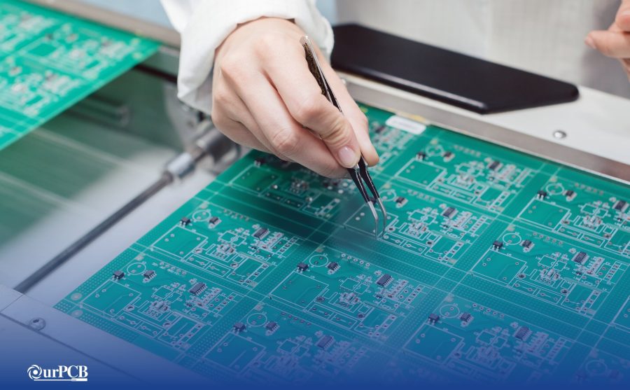
(PCB production under progress)
5. Advantages of Type 3 PCB Manufacturing
Class 3 circuit boards are essential in keeping planes in the air, individuals alive, and businesses to stay in place. So, Class 3 boards are a must when reliability and extended lifetime of a product are necessary. The following are some of the advantages that come with type 3 PCB manufacturing.
-
Design aspect
Class 3 boards undergo their procedure under tight specifications. Thus, users of this equipment enjoy the assurance of high-quality and long-lasting products. Their design is precise, careful, and up to the required industry-standards.
-
Manufacturing aspects
The manufacturing process of Class 3 tends to be different from that of Class 2. The manufacturing process of Class 3 products is a bit detailed compared to Class 2 products. While this process may be slow, in the end, it brings about perfect boards consisting of well-aligned parts.
-
Inspection aspect
When it comes to inspection matters, you’ll notice that Class 3 passes through rigorous inspection. While others may argue that this is expensive, manufacturers will avoid costs associated with recalls due to faulty products in the long run. A thorough inspection ensures the identification of faults early before full production. With such, the company will gain the trust of their customers based on high-performing equipment.

(A factory worker assembling a PCB)
6. What is the difference between assembling Class 2 and Class 3?
As mentioned earlier, Class 2 products are of a slightly lower quality compared to Class 3 products. In other words, the higher the number of the Class, the better its level of quality. So, what’s the difference between the assembly processes of Class 2 and Class 3 products? The following are the three significant differences:
6.1 The cleanliness and installation components are different.
A significant difference between the two courses is the rigor and quality they will endure. So, cleanliness and the installation of components between the two of them are different.
Since Class 3 products find heavy use in military and medical applications, they need a thorough cleaning. Also, the careful installation of its components is mandatory as compared to Class 2.
6.2 Class 3 assembly is more refined than Class 2
As mentioned above, Class 3 products are much reliable and have a very long lifespan. They are also perfect for high-reliability electronic devices. For this reason, it means that their assembly process is somewhat refined compared to Class 2.
These products need a careful and detailed assembly process. They are responsible for keeping planes in the air and the sick alive. Thus, the assembly process has to be exhaustive, unlike Class 2 products. For Class 3 products, there are no imperfections or missteps in the assembly process.
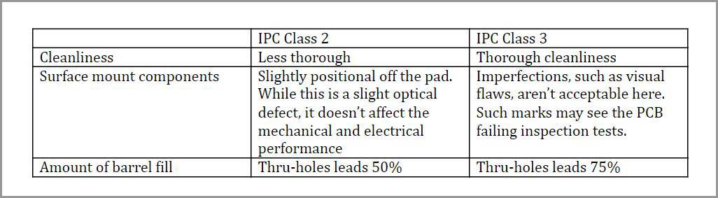
6.3 The difference in the barrel fill levels
Finally, another differentiating factor between Class 3 and Class 2 products regards the complete barrel fill that designers use in the thru-hole leads. Class 2 products consume less barrel fill (50%) than the 75% used by Class 3 products. It is a very delicate process getting the required amount of paste to small plated through-holes.
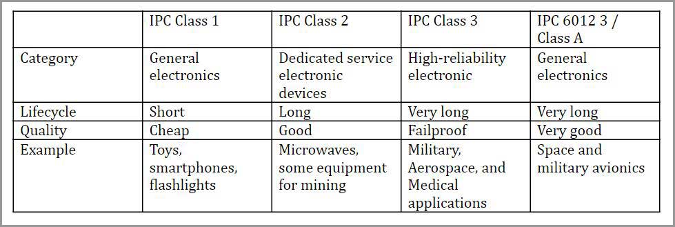
The table below provides a better visual understanding of the difference between Class 2 and Class 3 products:

(Factory workers assembling PCBs)
Special Offer: Get $100 off your order!
Email [email protected] to get started!
7. The Differences Between Class 2 and Class 3 for Printed Circuit Board Manufacturing
The following encompasses some of the most notable differences between Class 2 and Class PCBs:
7.1 Annular ring and drill breakout
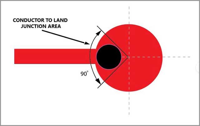
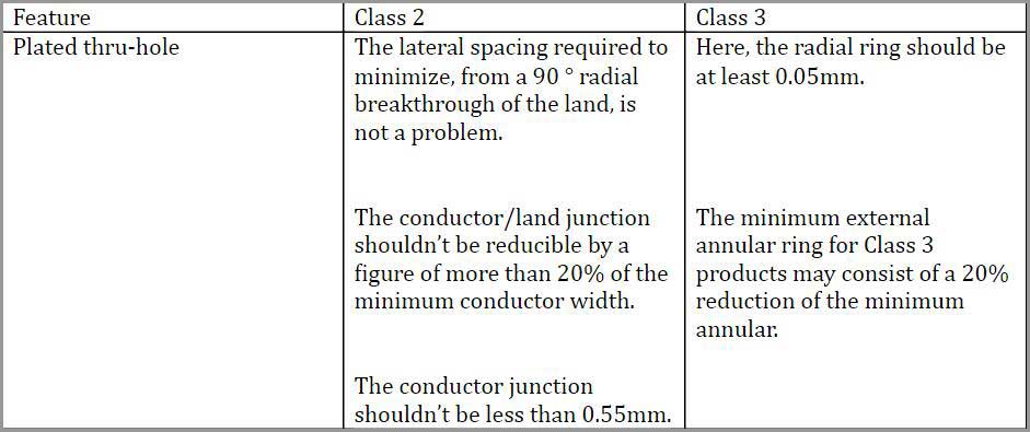
Another differentiating area between Class 2 and Class 3 is on drill breakouts. PCBs in the Class 2 category allow breakouts to occur from the annular rings. However, Class 3 does not permit fractured annular rings.
PCBs that fall under Class 3 needs to be very resilient. It means that there won’t be significant damage to the entire board if there’s a breakout. When dealing with Class 2 products, having a 90° escape is not a problem if you maintain minimal spacing on the lateral sides.

7.2 IPC annular ring acceptance criteria
The following table better highlights the IPC annular acceptance criteria between Class 2 and Class 3 products. The IPC annular ring acceptance criteria is another differentiating factor between Class 2 and Class 3 products.
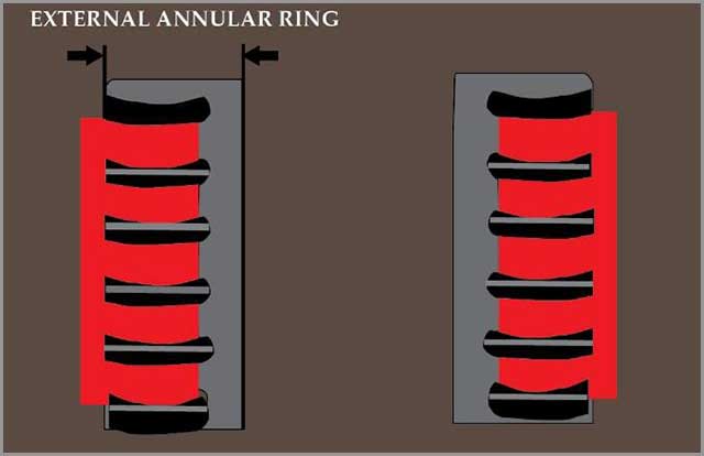
7.3 Design rules of annular rings
The required acceptance for Class 2 and Class 3 is necessary for better board functionality. The tables below better explain essential matters to do with the design rules of annular rings:
7.3.1 IPC Class 2 Drill and Pad Diameter for 1/2 oz Copper
| Drill | Pad | Anti-Pad | PCB Thickness | Aspect Ratio |
| 0.006'' | 0.016'' | 0.026'' | Up to 0.039'' | 6.5:1 |
| 0.008'' | 0.018'' | 0.028'' | Up to 0.062'' | 7.75:1 |
| 0.010'' | 0.020'' | 0.030'' | Up to 0.100'' | 10:01 |
| 0.012'' | 0.022'' | 0.032'' | Up to 0.120'' | 10:01 |
| 0.0135'' | 0.024'' | 0.034'' | Up to 0.135'' | 10:01 |
7.3.2 IPC Class 3 Drill & Pad Diameter for 1/2 oz Copper
| Drill | Pad | Anti-Pad | PCB Thickness | Aspect Ratio |
| 0.008'' | 0.023'' | 0.033'' | Up to 0.062'' | 7.75:1 |
| 0.010'' | 0.025'' | 0.035'' | Up to 0.100'' | 10:01 |
| 0.012'' | 0.027'' | 0.037'' | Up to 0.120'' | 10:01 |
| 0.0135'' | 0.028'' | 0.038'' | Up to 0.135'' | 10:01 |
7.3.3 And these tables are for various copper thickness:
| Drill & Pad Diameter | 8 Layers or Less | >8 Layers | ||||||
| IPC Class 2 | Pad Diameter Over Drill | Pad Diameter Over Drill | ||||||
| 1/4 oz Copper | 0.010'' | 0.010'' | ||||||
| 3/8 oz Copper | 0.010'' | 0.010'' | ||||||
| 1/2 oz Copper | 0.010'' | 0.010'' | ||||||
| 1 oz Copper | 0.012'' | 0.012'' | ||||||
| 2 oz Copper | 0.014'' | 0.014'' | ||||||
| 3 oz Copper | 0.016'' | 0.016'' | ||||||
| 4 oz Copper | 0.018'' | 0.018'' | ||||||
| Drill and Pad Diameter | 8 Layers or Less | >8 Layers | Drill and Pad Diameter | 8 Layers or Less | >8 Layers | |||
| IPC Class 2 | Pad Diameter Over Drill | Pad Diameter Over Drill | IPC Class 3A | Pad Diameter Over Drill | Pad Diameter Over Drill | |||
| 1/4 oz Copper | 0.013'' | 0.015'' | ||||||
| 3/8 oz Copper | 0.013'' | 0.015'' | ||||||
| 1/2 oz Copper | 0.013'' | 0.015'' | 1/2 oz Copper | 0.013'' | 0.015'' | |||
| 1 oz Copper | 0.015'' | 0.017'' | 1 oz Copper | 0.015'' | 0.017'' | |||
| 2 oz Copper | 0.016'' | 0.018'' | 2 oz Copper | 0.016'' | 0.018'' | |||
| 3 oz Copper | 0.019'' | 0.021'' | ||||||
| 4 oz Copper | 0.022” | 0.024” | ||||||
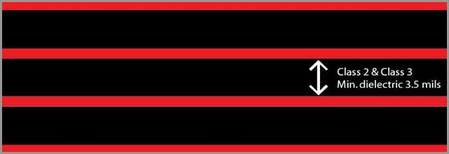
7.4 PCB dielectric requirements
According to industry standards, the minimum dielectric rule for Class 2 and Class 3 should be 3.5 mils. Anything above or below that figure is just substandard.
7.5 PCB through-hole plating requirements
Class 3 products tend to be slightly astringent, especially for copper voids. Copper voids are situations where copper plating in the hole’s barrel isn’t there. It tends to leave the drilled hole’s dielectric material exposed. On the other hand, Class 2 gives an allowance of 5% significant chance of a single void in the board’s gaps. When it comes to plating thickness requirements, Class 2 needs 0.8mil while Class 3 is one mil.
The above are, but a few issues that make Class 2 and Class 3 differ. But as usual, we would always advise you to seek communication with your producer. They can better guide you to resolve all upcoming issues, and they will do it right. Also, don’t forget to request some cross-section of your PCB. By doing this, you’ll be ensuring that your producer met either your Class 2 or Class 3 requirements, as you had earlier requested.
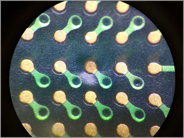
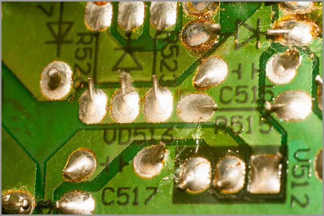
(PCB pads on an isolated black background)
8. How to Quickly Design your IPC PCB
IPC PCBs are PCBs manufactured in the required way. These printed circuits boards are safe to use, reliable, and of the highest quality. It is because IPC standards compel manufacturers to produce safe, high-quality, high-performing PCBs.
IPC standards ensure that manufacturers maintain the quality and reliability of their products. Also, it ensures that manufacturers maintain consistency, better communication, and cost reduction. So, how do you go about quickly designing an IPC PCB? It’s not as complicated as you may imagine.
Let’s highlight them:
- First, ensure your land and specifications of spacing are within the recommended tolerances.
- Second, make sure that the entire drill holes do meet the size and all the quality requirements. Also, make sure that they align with all the aspect ratios of your contract manufacturer’s equipment.
- Third, ensure that the solder mask specifications do fall with the recommended tolerances. If you design class A products, then the solder mask specifications must meet its class’ tolerances. The same is for Class 1, 2, or 3 products.
- Fourth, you need to make sure that your contract manufacturer does apply high-quality control. Such would include exercises such as AOI inspections in the entire fabrication and later in the assembly process.
- Next, ensure that the contract manufacturer that you choose prioritizes cleanliness. You do not want to purchase unclean boards that are full of debris. Such may end up affecting the functionality of your devices.
- Lastly, you may have to apply Class 3 specifications for the entire board properties unless otherwise stated.
Adherence to IPC standards is necessary if you want your functional boards. Then, it would help if you had a manufacturer that can meet the required regulatory requirements. But as you can see, designing IPC printed circuit boards is not a complicated process as such.
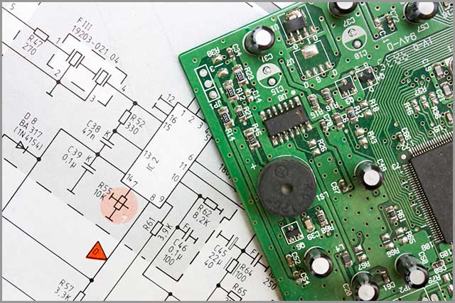
(Schematic diagram of a PCB design)
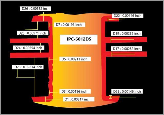
9. PCB Specification Verification-cross-sectional area
It's not easy to ensure the integrity of PCBs without subjecting them to cross-sectional examination. Cross-sectioning is a metallographic technique that designers use to characterize the materials and perform a PCB’s performance failure analysis. The following are the four most common PCB specification verification analysis.
9.1 Judgment criteria
A judgment criterion is essential to ensure that only the best entry gets to win. Before a PCB hits the shelves, they need careful examination by designers. When it comes to PCBs, judgment criteria involve assessing areas such as solder joint issues, flux residues, lifted components, and blowholes, to mention but a few.
9.2 Cross-section standard for Class 2
Cross-section standard for Class 2 checks for a variety of things on a printed circuit board. Manufacturers need to subject Class 2 PCBs to such analysis to identify the following:
- The thickness of the surface finish
- The connection that exists between the layers
- The thickness of the copper
- The registration of both the internal and external parts
- The plating thickness of hole-wall in plated through-hole
9.3 Class 3 cross-section standard
As mentioned way earlier, Class 3 products are those high-performing electronic products. They must offer continued performance for a long without showing signs of fatigue. But just like its counterparts, cross-sectional verification is also a rule here. Cross-section analysis checks for aspects like solder mask width, plasma etch, plating, copper, and dielectric.
9.4 3A-level cross-section standards
Lastly, there are 3A-level cross-section standards. These are high-level cross-section standards, much higher than class 3 cross-section standards. They check for all aspects on the board in totality, not a single section, but everything.
10. IPC defects in PCB
Even though IPC PCBs are some of the best in the market, they are also prone to defects. Manufacturers may make some errors during production. These errors may affect the entire equipment’s functionality. The following are some of the most common IPC defects in PCB:
-
Annular ring:
The annular ring is the copper pad area located around a drilled and finished hole. Defects around the annular ring is a common IPC PCB defect. IPC PCB annular ring defects come in as one primary concern for PCB designers. However, some acceptable standards (such as a 90-degrees breakout on the annular ring) won’t affect the board’s performance.
-
Solder joint:
Solder point is another major IPC defect in printed circuit boards. The solder joint defects do happen if the joint did not heat enough. It may also take place if the soldering iron is at a shallow temperature.
Solder collective faults look messy and don’t last long. At times, solder point defects affect the functionality of the PCB.
The best way of avoiding such a problem is to ensure the best soldering techniques. There’s no specification for Class 1. But, Class 2 and 3 need 180 degrees and 270 degrees, respectively.
-
Component misalignment:
This is equally another IPC defect found in printed circuit boards. It takes place the moment a PCB gets inappropriately positioned to the target area. Components misalignment takes place when components tend to float on molten solder. IPC guidelines when it comes to components misalignment are:
- Type 1-less than 50% of the terminal or land width,
- Level 2-Less than 50% of the terminal or land width,
- Level 3-Less than 25% of the terminal or land width.
At times, there aren’t any specifications for Class 1 as such, but several guidelines for Classes 2 and 3. Sometimes, all three classes do share the same requirements for defects. It’s imperative to understand the needs of each standard to meet the desired design objectives.
(A solder joint defect on a PCB)
11. Inspection Standard / IPC Standard Compliance
IPC (Institute for Printed Circuits) is the official name of the organization that formulates PCB-related standards. Before the change of name, the association was the Institute for Printed Circuits. While it currently goes by the Association Connecting Electronics Industries’ name, it still retains the IPC moniker.
In itself, the IPC is an association of international industries with more than 4,000 members. Their function is to make then use, specify, and design PCBAs including:
- Computer
- Industrial equipment
- Telecommunications industry
- Medical and equipment services
- Advanced microelectronics
- Automotive
Therefore, we have IPC standards in place. These electronics industries need to use standard PCB designs, manufacturing, and assembly. Regardless of whether one works in manufacturing, defense, or electronics design, IPC compliance is necessary. IPC standards come in as some of the most accepted PCB design standards globally.
But what’s the importance of compliance?
Are there any benefits that come with complying with such standards? For PCB designers, observation is crucial, based on several reasons. For instance, PCB firms that follow such standards prove reliable, accountable, and credible.
Compliance also passes the message that PCB manufacturers only produce safe and high-quality PCBs. With this, producers reassure their end users that the products will function as intended. By complying with IPC standards, PCB producers join hands together, eliminating any confusion, speeding up verification, and ultimately reducing costs.
IPC standard compliance measures keep manufacturer of printed circuit boards in check. Such standards ensure that PCB manufacturers produce safe and durable PCBs. Companies that follow such standards avoid unnecessary legal battles. These legalities include lawsuits for manufacturing environment-unfriendly.
In short, compliance comes with plenty of advantages, especially for PCB suppliers. Besides gaining their customers’ trust, it shows that such firms are accountable and reputable.
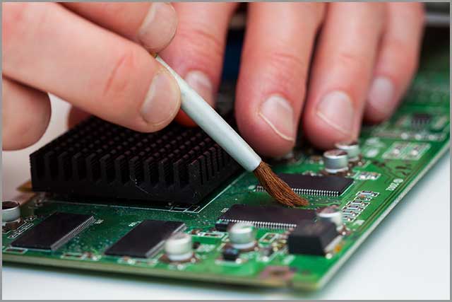
(Cleaning a PCB for IPC compliance)
12. Precautions for IPC Products
IPC products aren’t in the same league as the rest. They have their standards, meaning that there’s a need to observe certain precautions when dealing with them. The following are four of the essential things to consider when it comes to IPC products:
12.1 Cost issues
The costs of PCBs are one of the biggest concerns for manufacturers. Certain factors lead to high costs of PCBs. Some of them include the type of material used, surface treatment, and panel size, to mention a few.
The same is true when it comes to IPC products. Since such products must meet specific standards, it means that their costs will be high. As a manufacturer, you may want to strike a balance between prices and quality. You shouldn’t compromise on quality over costs. As a customer, you need to understand that cheap may turn out to be expensive.
The cost is a big issue when it comes to IPC products. As a producer of IPC products, ensure that you find the perfect balance between prices and quality.
12.2 Impact of Through-Hole Technology
Even though through-hole technology (THT) seems to be losing popularity, there are certain situations where THT is the best choice. Rarely do PCBA designs use THT today. However, there THT is suitable in extreme cases like space and industrial applications. Even though through-hole isn’t that popular, specific IPC standards guide them.
With THAT, IPC needs to meet specific IPC standards, especially ones to do with THT PCB layout. An apt example is the drill hole size. Here, it’s the duty of contract manufacturers to boreholes that their customers need. Also, the aspect ratio meets the board’s requirements to avoid altering structural integrity. In terms of the annular rings, IPC standards state that annular rings diameter needs to be enough. The reason for this is to ensure that it brings out excellent solder joints.
12.3 Surface Mount Technology
SMT is a technology that involves mounting electrical components on a PCB’s bare surface. The electrical components that sit onto the PCB surface are SMDs or Surface Mount Devices. Certain IPC precautions relate to Surface Mount Technology.
For instance, IPC-DRM-18 highlights the identification and subsequent place of components. It is vital to ensure that component placement follows the right procedures. The correct order of SMD components ensures the longevity and reliability of circuit boards.
12.4 Literature
People have said a lot on matters to do with IPC products. Some information is accurate while there are half-truths, and many lie on PCB products. It would help if you were cautious when going through IPC literature. Make sure that you get such information from credible sources only.
13. Do you Want to Build an IPC Class Project?
Now that you’ve read almost everything on IPC products, you may want to try building one for yourself. There’s no harm in trying a DIY project. In the end, such an exercise may end up being fun and a chance for you to learn something new. Unfortunately, though, such a project may be daunting at first, if not confusing. For this reason, you may need the services. If you find yourself in such a situation, do either one or both of the following:
-
Choose high-quality designers
For the best IPC products, you may have to go for high-quality designers. Of importance to note is that not designers are who they say they are. Some are in business to fleece you of the money you spent so hard earning. If you want the best IPC products, conduct a little background check on your potential designer(s). What are people saying about the quality of their goods? If the reviews are negative, then you better look elsewhere. It’s that simple. For the best result, partner with the best designers in the field.
-
Look for a high-quality PCB production service company.
There are hundreds of PCB production companies currently in business. Sadly, not all guarantee you high-quality products. A good number of them are new in a place and still learning the ropes. Much worse, very few of them can successfully meet all your PCB needs the way you want. Finding a high-quality PCB production company isn’t a laborious process as such. You may inquire from friends or look up on the internet to find reliable ones.

(A team of PCB electronic designers at work)
Summary
Ensuring that your board’s manufacturer complies with all IPC standards for PCBA is more than whether your board falls in Class 1, 2, or 3 categories. The right way to ensure IPC standards is by following the keys to a good PCBA design. Among other things, such would include establishing an early relationship with qualified CM’s.
We will ensure that we work with you, ensuring that your boards do adhere to IPC standards. Do you need more information about IPC standards meant for PCBA? Feel free to contact us for help.
Special Offer: Get $100 off your order!
Email [email protected] to get started!