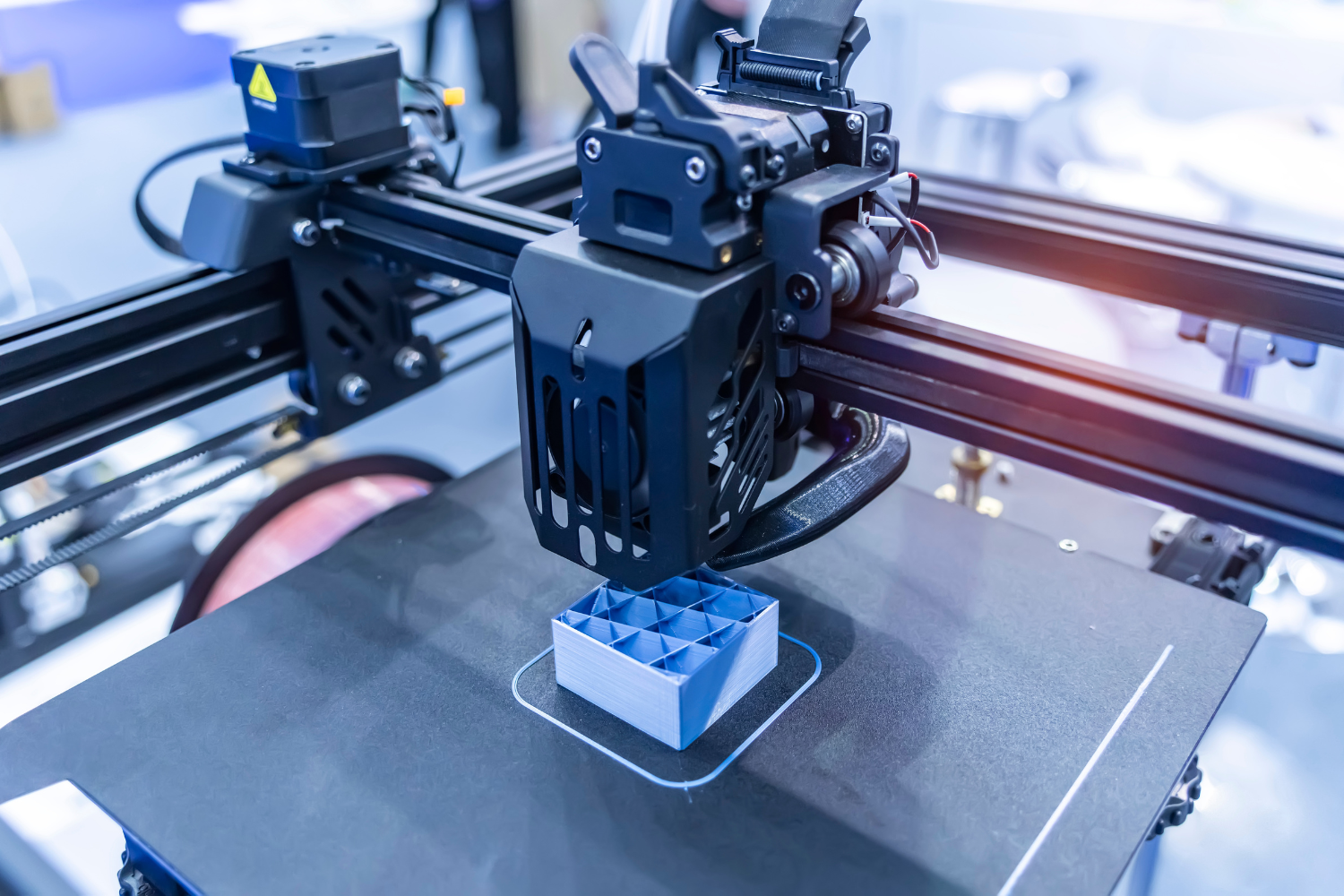
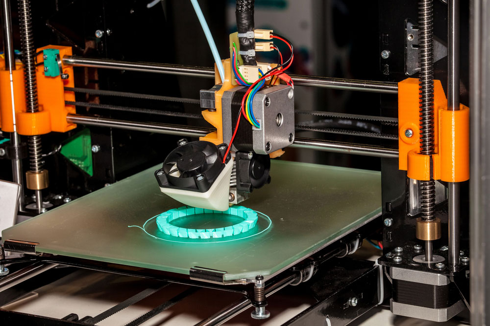
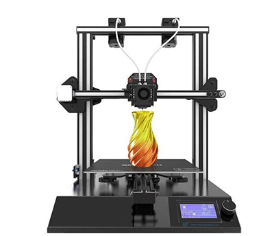
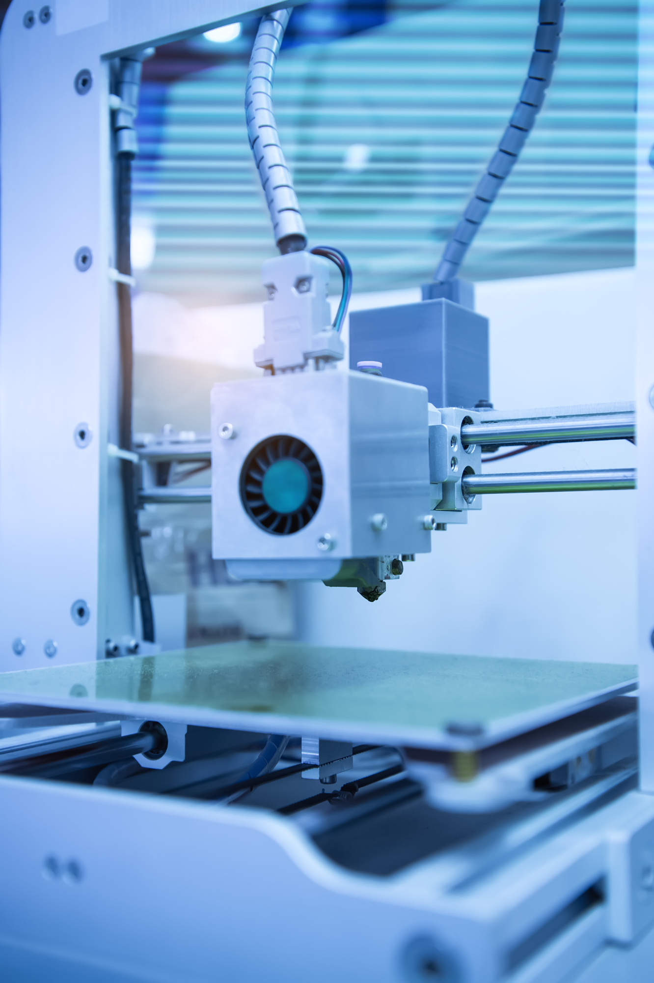
Blog  /  A Beginner’s Guide to Designing and Printing 3D Circuit Boards

A Beginner’s Guide to Designing and Printing 3D Circuit Boards

Traditional methods of circuit board fabrication are costly and quite limiting in terms of scale and design complexity. Also, they can be wasteful because laser cutting and CNC milling cut off unwanted sections. However, the PCB 3D printing process can layer large and complex custom PCBs affordably while reducing wastage. These benefits enable hobbyists and DIYers to build 3D printed circuit boards from the comfort of their homes. We have covered these circuit boards in detail below and if you need one for your project, read on to learn more!

What is a 3D Printed Circuit Board? Why Use It?

A 3D printed circuit board is a PCB made using an additive process that creates the 3D solid board from a digital design file. Most traditional PCB fabrication processes involve CNC milling, laser cutting, or ironing on glossy paper. However, with the PCB 3D printing process, you make circuit boards by laying the conductive or hollow traces first. The only difference is in the fabrication process, but these finished boards appear and function like regular PCBs.

A 3D printer

A 3D printer

Do 3D Printed PCBs Work? Can They Replace Regular PCBs?

3D printing circuit boards work, but the technology is not ripe enough to replace regular PCBs. Otherwise, we wouldn’t be having these boards made using the subtractive process.

The primary limitation of these boards is in the conductive layer. Printers used for this process cannot melt copper and layer it on the board. In fact, the only way to additively layer the traces is to melt the copper and pour it into thin strips using a thin nozzle.

Two engineers assessing a 3D PCB concept on a computer

Two engineers assessing a 3D PCB concept on a computer

Molten copper can damage the substrate because it is hotter than the material’s melting point. But more importantly, the metal’s high thermal conductivity means it dissipates heat severely when being printed, which results in mechanical and dimensional variations.

You can mix copper with other metals, but the alloy might not have the required electrical properties for high-speed or high-frequency transmission.

Therefore, the only option is to lay out the electrical lines using conductive PLA filament or metal-infused ink. These types of transmission lines are not good enough for demanding applications like RF PCBs.

Applications of 3D PCBs

Phased array antennas require 3D printers to layer the complex, multilayer circuit on curved surfaces. This process is expensive because regular materials are insufficient for high-frequency applications.

Other radio frequency systems, like radar systems, are also benefiting from 3D printing because the technology reduces their production time and manufacturing cost, while eliminating the fabrication complexity.

3D PCBs are ideal for biomedical research, as well, because they make it easier to build complex and delicate circuits that must include components like stretchable sensors and connectors.

This technology is also suitable for additive layering of solar cells on Fz wafers. 3D printers can lay silver-infused ink in narrow lines (18-60 microns in width) to form the collector lines.

Methods to Make 3D Printed Circuit Boards

There are several methods of creating 3D print circuit boards, but the two primary ones are:

Using Conductive Filament

This method involves using the 3D printer to lay down the conductive element first, creating line patterns similar to those found on a regular PCB.

You can use other materials to develop multiple layers with conductive filament printing. Also, you can create different PCB shapes, not only the usual flat surface.

The typical filament materials used for printing are conductive inks or TPU, ABS, HIPS, and PLA with graphene. Filament printing forms the board only on which you can solder electronic components.


Creating Hollow Traces

The second method is the opposite of conductive filament printing. Creating hollow traces involves printing the solid block with conductive trace channels formed internally. Afterward, you can fill the slots with conductive material, such as conductive epoxy resin or electric paint.


Creating hollow traces is easier and quicker than using a conductive filament because it doesn't require post-production soldering. However, the process is less capable of creating complex high-density-component designs.

How Do You Print a Circuit Board on a 3D Printer at Home?

You’ll need the following components for this printing process.

  • Dual-extruder 3D printer
  • Non-conductive and conductive PLA filaments (the latter should be graphene or carbon black)
  • Cold solder adhesive
  • CAD design software
  • PCB2STL file conversion software

Step 1: Set Up the 3D Printer

Calibrate the printer by making sure the printing bed is perfectly level, and the height of the two extruders is the same from the bed. Also, load the two filaments, each on its extruder.

When buying them, ensure the conductive filament has a resistance of less than one ohm per cubic centimeter to be effective. We recommend the graphene type because it is more conductive than carbon black.

Two engineering students working on a 3D printing project (one is calibrating the machine)

Two engineering students working on a 3D printing project (one is calibrating the machine)

Step 2: Finalize and Save the PCB Design

Whether you use free or premium CAD software, finalize the board’s design and then export the Gerber file.

You’ll need individual Gerber files for the copper layers, edge cuts, plated-through drill holes, and non-plated-through drill holes.

Step 3: Check Your 3D Model

Upload your 2D Gerber files to the PCB2STL file conversion software, which will convert them into 3D models.

The program should give you two STL files for your 3D printer, one for each extruder. Although these STL file outputs are hole-free and have manifold faces, check them to ensure everything is in order.

Step 4: Load the 3D Model to Your Printer

Load the 3D model into the 3D printer and slice it to separate the design into executable instructions that the device can understand (G code). The two STL files must be perfectly aligned to have a common point of origin for the two extruders.

Step 5: 3D Print the PCB

Start the printing process and give it some time to complete. The standard board thickness is around 1.6mm, and the PCB2STL conversion software only supports rectangular and square boards.

If you want your 3D board in another shape, you can cut the flat board and glue it in another configuration.

Step 6: Assemble the PCB

You cannot solder this board the regular way; hot solder will melt the polyester substrate. The next best solution is to use cold soldering, which involves applying a conductive adhesive to hold and connect the component pins to the circuit.

Conductive granite ink on an LED circuit

Conductive granite ink on an LED circuit

You can use a circuit writer pen, which has silver glue, and write around the pads and pins several times to get the glue in there. Afterward, test the assembled board to check if the circuit works.

The Best Desktop 3D PCB Printers

Some of the best 3D printers in the market include the following.

Voltera V-One PCB Printer

The Voltera V-One is an ideal entry-level 3D PCB printer because it is relatively affordable (slightly above $2,000). Despite its low price, the device has a decent build volume and can print boards measuring up to 135 x 113.5mm. Additionally, it is compatible with several CAD software packages.


V-One can layer a 0.8mm pin-to-pin minimum pitch with conductive ink and a 0.6mm minimum pitch with solder paste. Regardless of the conductive trace, the width cannot be less than 200 μm.

Nano Dimension DragonFly 2020 PCB Printer

Heralded as the first 3D printer in the world, the DragonFly 2020 is the first of its kind to adhere to IPC guidelines. The unit can fabricate PCBs with the following properties.

  • 25μm positional accuracy on any axis
  • 200 x 3 x 200 mm maximum build size
  • Min & max feature sizes of 80 μm & 1.5mm, respectively
  • 0.03 mm or 30 μm minimum layer thickness
  • Multilayered boards with 3mm total thickness


The printer supports conductive and dielectric polymer inks for hollow traces. However, it is expensive because prices start at $50,000.

Othermill Pro PCB Printer

The Othermill Pro printer is a precise, portable milling machine built to produce double-sided circuit boards as thin as 150 μm trace widths. It can create PCBs measuring 140 x 114 mm maximum with a 75 μm positional accuracy. Even though it is affordable, the machine cannot work with hard materials like FR-4 and glass, and it is available only in the US. However, it is compatible with several OSs and CAD software.


Voxel8 PCB Printer

One unique feature of this Voxel8 printer is its dual print heads. The first one uses silver (conductive) ink, while the other uses fused wire based on the typical FFF/FDM technology.

Each ink head features a 250-micron diameter nozzle, and the print bed is magnetic for high repeatability. This bed allows you to remove the incomplete object temporarily while printing to insert components, then resume the process.


Squink by BotFactory

Squink's unique selling point is that it can print multilayer boards on different rigid and flexible substrates with a max size of 84 x 152 mm. However, it can print larger single-layer boards, with the maximum size being 152 x 152 mm. The recommended feature printing size is 0.508mm, but it can go as low as 0.254mm.

A 3D printer

A 3D printer

The printer contains three heads, one for printing, the second for gluing, and the third for picking & placing. Besides printing, the unit can assemble four parts per minute, with the tiniest package size being 15.4mm. However, the machine cannot place thru-hole components automatically.

Cool 3D Printing Projects

Electric Coffee Maker with 3D Printed Parts

An electric coffee maker contains several parts & connectors, and it is easier to order the internal components. However, you can design and 3D print the casing parts individually. With all the pieces ready, assemble the coffee maker and try your new appliance.

3D Printed Telescope

3D printing a telescope requires some skills and knowledge. Downloading and printing the parts is easy, but mounting the mirror and assembling the camera & focus can be challenging. Also, you need a Raspberry Pi to control the camera.


Loudspeaker iPhone Extension

If you prefer listening to music from your iPhone without using earbuds or headphones, a 3D-printed loudspeaker can help amplify the sound.

The loudspeaker will have echoing chambers on both sides that raise the sound level. You can use these design files for an iPhone 6 and 6+.

Benefits & Drawbacks of 3D Printed Circuit Boards

3D PCBs have the following advantages and disadvantages.

Edges of 3D Printed Circuit Boards

Quick Production: 3D PCB printing ensures computers handle the design and fabrication processes. This operation hastens the production time to enhance efficiency and increase capacity.

Less Waste Material: Unlike traditional methods that mill or corrode the excess material, 3D printing is a deposition method that only utilizes the required material. Therefore, it wastes less, translating to high-cost savings.

Greater Design Flexibility: Computer-Aided Design gives you high flexibility. Thus, you can experiment with different layers, forms, or shapes when making circuit boards for various industries.

Limitations of PCB 3D Printing

  • Less Effective Conductive Materials: The conductive paint or epoxy resin used to make electrical paths in hollow trace printing is not as effective as metal. The electrical resistance of these materials can be a problem depending on your project's scale.
  • Risky When Soldering: Soldering is necessary when using conductive filament printing. Depositing molten metal to the board can weaken it significantly. Remember, soldering irons can hit 300°C, and such temperatures can damage the printed metal.
  • Lack of Software Support: CAD programs can be costly. However, there are open-source design applications that are free to use. But these usually lack support or guidance. Therefore, it can be challenging to try 3D circuit board design and printing (unless you have some design experience).


Automated 3D Printed Circuit Board Print.

Once you get the hang of it, you should be able to 3D print the plastic board and deposit the conductive material or solder simultaneously.

Doing so should create the complete PCB in one or two rounds. The process involves printing a component holder, inserting the components, then printing the board & its conductive traces to complete the circuit.

State of 3D Printed PCBs

Printed circuits have traditionally been on boards, which can be rigid or flexible flat 2D structures. But with 3D printing, you can create a circuit on any board shape in 2D or 3D form.

This flexibility means you can create a honeycomb or cylinder-shaped circuit in a rigid form to fit into tight spaces while providing enough circuitry and components for the specific function.

You can use flexible PCBs, but these have several limitations over their rigid counterparts, a key one being a weaker, less durable structure.

Once this capability is available for commercial use, manufacturers of biomedical devices like wearables and implantables will be able to fabricate tinier devices to fit seamlessly in the body.

Another state of 3D printing that will have a significant impact on manufacturing is the additive printing process.

Traditional circuit boards go through etching, a subtractive manufacturing process, to eliminate excess copper from the foil to form the signal lines or traces.

But 3D printing is an additive process, which means it requires less energy and fewer materials, creates less waste, and is less harmful to the environment because you don’t have to use corrosive chemicals.

Summary

In conclusion, 3D circuit boards significantly reduce the costs of prototyping and developing DIY projects. Buying a 3D PCB printer can be costly but worth it. Also, you need to learn Computer Aided Design.

But once done, you will cut production time by a wide margin. That's it for this article. If you have any questions or comments, leave a message, and we'll get back to you in no time.