


ISO 9001/UL Certified
PCB Assembly Specialists
97% of PCB Shipped on Time
98% of PCB Delivered to Spec
Delivery Guarantee

Online Quote

Upload PCB File

Order Review

Payment

Order Updates

Delivery

Confirm Received

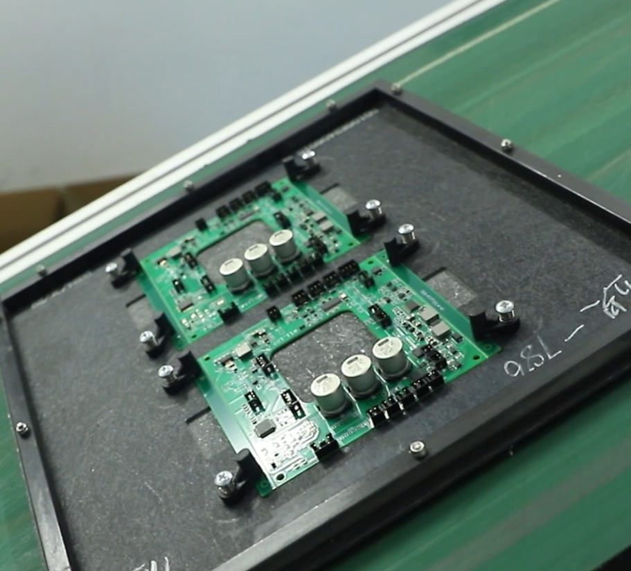
Quality Assurance
- Rigorous testing ensures each board meets high standards
- We use advanced equipment for precise fabrication
Flexible Options
- Choose from various board materials and finishes
- We offer both single and double-sided PCBs

Cost-Effective Solutions
- Competitive pricing for small batch orders
- No minimum order quantity for prototypes
Expert Support
- Our team provides guidance on design and fabrication
- We offer resources to help improve your PCB designs
Design Freedom
- Create boards that fit your specific project needs
- Experiment with different layouts and components
Learning Opportunity
- Gain hands-on experience with PCB design and fabrication
- Understand the full process of electronic product development
Cost Savings
- Avoid the high costs of mass-produced boards for small projects
- Iterate designs without large financial commitments
Customization
- Add personal touches like custom silkscreen designs
- Choose specific materials or finishes for your board

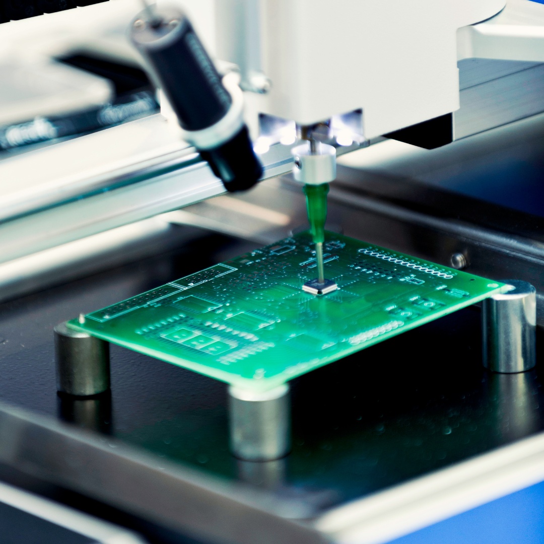
SMT Assembly
- We use SMT for compact, high-performance boards
- Our equipment can place tiny components with precision
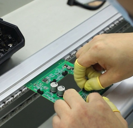
Consigned Components or Turnkey PCB Assembly
- We work with your supplied parts or source components
- Our turnkey service covers everything from parts to final product
Custom PCB Assembly
- We adapt our process to your unique board designs
- Our team can handle special requirements or unusual layouts
Quick Turn PCB Assembly
- We offer quick assembly services without sacrificing quality
- Our efficient process helps you meet tight project deadlines
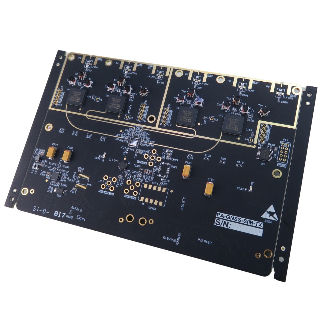
IPC Class 3 PCB Assembly
- We follow strict quality guidelines for critical applications
- Our assemblies meet aerospace and medical industry standards
All IC Packages PCB Assembly
- We can assemble all types of IC packages
- Our expertise covers BGAs, QFNs, CSPs, and more
Chat with Us
Mon-Fri: 24 hours,
Sat: 9am-6pm, GMT+8
Email Us
Reach us at
[email protected]
24 hours online
Call us
+86-199-30589219
Mon-Fri: 24 hours,
Sat: 9am-6pm, GMT+8

